High Purity SiC Powder: A Deep Dive into Crystal Growth Performance
In the competitive landscape of third-generation semiconductor manufacturing, the quality of raw materials fundamentally determines crystal growth outcomes. High purity silicon carbide (SiC) powder has emerged as a critical bottleneck material for Physical Vapor Transport (PVT) crystal growth processes. This comprehensive review examines the performance characteristics, market validation, and differentiated value propositions of advanced high purity SiC powder solutions currently transforming the industry.
Understanding the Critical Role of SiC Powder Purity
Silicon carbide crystal growth via the PVT method operates at extreme temperatures exceeding 2000°C, where even trace impurities can trigger catastrophic defects. Traditional Acheson-process SiC powder—the conventional industry standard—has long plagued manufacturers with two fundamental problems: excessive nitrogen contamination that introduces unwanted doping effects, and progressive graphitization during extended growth cycles that releases carbon inclusions into the crystal lattice. These contamination pathways directly translate to micropipe defects, etch pits, and wafer scrap rates that erode profitability.
The technical specifications demanded by modern 6-inch and 8-inch SiC wafer production have driven material purity requirements to unprecedented levels. Industry leaders now specify 7N purity standards (99.99999% silicon carbide content) with nitrogen concentrations below 5×10¹⁵ atoms/cm³ and total metallic impurities under 5 parts per million. Meeting these thresholds requires fundamentally different production methodologies than traditional carbothermal reduction processes can deliver.
Chemical Vapor Deposition: The Purity Breakthrough
Advanced manufacturers have pioneered CVD-derived polycrystalline SiC powder as the solution to conventional powder limitations. Unlike Acheson powder produced through high-temperature reactions between silica sand and petroleum coke—which inherently carries nitrogen and metallic contamination from raw materials—CVD synthesis builds silicon carbide structures atom-by-atom from ultra-pure gaseous precursors in controlled reactor environments.
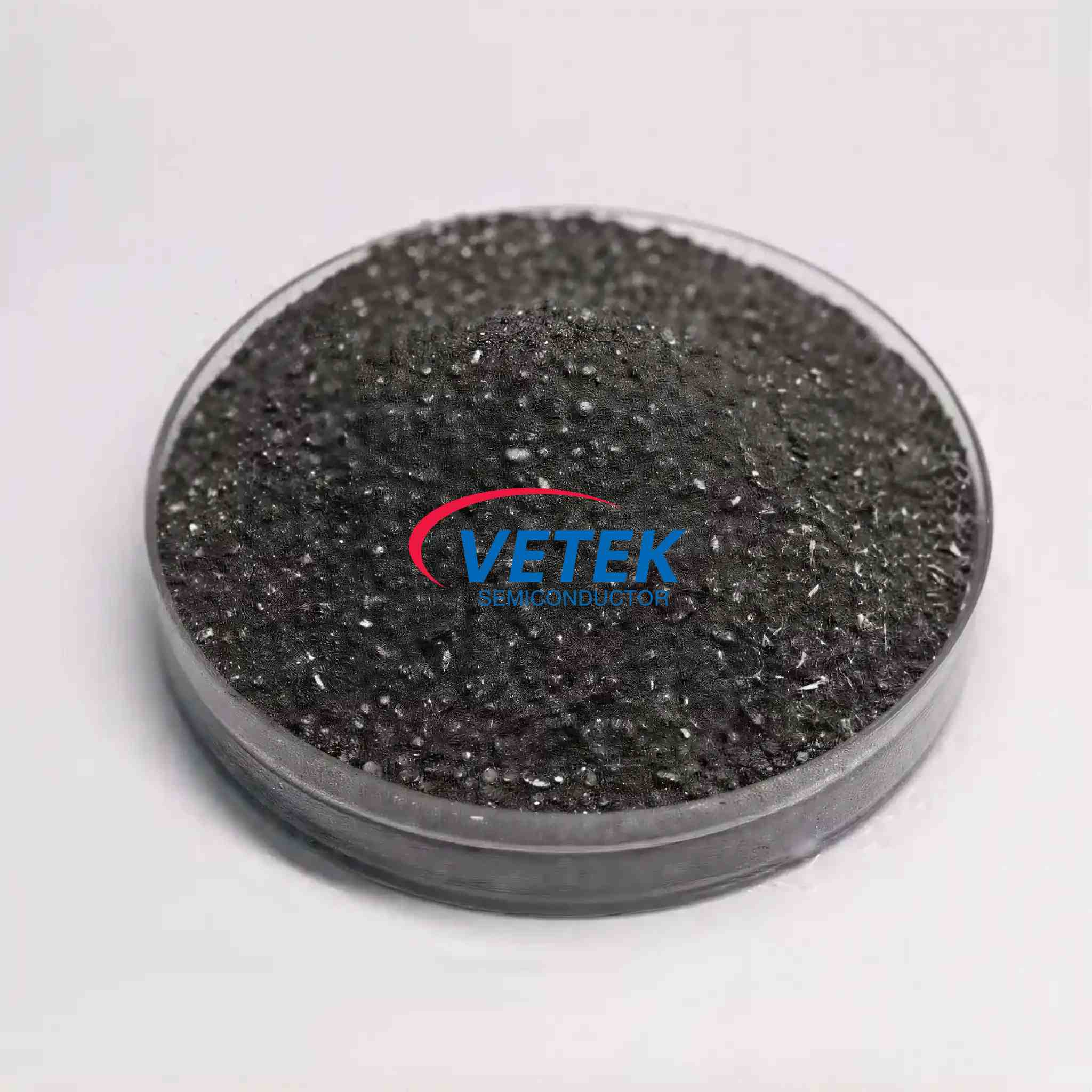
VeTek Semiconductor's proprietary CVD SiC raw material exemplifies this technological leap. The production process yields large-grain polycrystalline blocks with total impurity content verified below 5ppm through Glow Discharge Mass Spectrometry (GDMS) analysis. Critical contamination elements including iron, nickel, copper, and aluminum are suppressed to sub-ppm levels, while nitrogen incorporation—the primary concern for electrical properties—is maintained below the 5×10¹⁵ atoms/cm³ threshold that enables intrinsic crystal behavior.
Particle Morphology Engineering for Crucible Optimization
Beyond chemical purity, physical characteristics of SiC powder profoundly impact growth efficiency and crystal quality. The grain size distribution and particle morphology determine crucible packing density, sublimation kinetics, and vapor phase stoichiometry throughout the multi-day growth cycle.
Advanced CVD SiC powders utilize 4-10mm grain sizes specifically engineered for optimal crucible loading. This particle size range achieves two critical advantages: First, larger grains enable higher packing density, allowing crucibles to accommodate approximately 1.5 kilograms more raw material compared to conventional fine powders. This extended source capacity supports longer growth runs without mid-cycle interruption. Second, the blocky morphology of CVD-derived grains resists the graphitization phenomenon that afflicts Acheson powder during extended high-temperature exposure, preventing late-stage carbon contamination that typically degrades crystal quality in the final growth phases.
Quantified Performance: Real-World Crystal Growth Validation
Market validation from leading third-generation semiconductor manufacturers provides compelling evidence of CVD SiC powder's performance advantages. SiCrystal, a Rohm Group subsidiary and global producer of SiC substrates for power electronics and RF applications, deployed VeTek's high purity CVD SiC powder in their PVT crystal growth furnaces. The implementation delivered measurable improvements across multiple quality metrics:
Extended crucible reuse cycles to 200 hours—a substantial increase over the 150-hour typical baseline with conventional powder—translating to reduced consumable costs and improved equipment utilization. The high-purity material achieved zero weight loss in the extreme thermal environments of the growth zone, confirming superior structural stability. Most critically, finished crystal analysis revealed reduced defect densities including lower micropipe counts and decreased etch pit density, directly improving wafer yield rates for downstream device manufacturers.
The technical mechanism behind these improvements centers on contamination control. Nitrogen impurities in conventional powder create unintentional n-type doping that disrupts the semi-insulating properties essential for high-voltage device applications. Metallic contaminants serve as nucleation sites for structural defects during crystal solidification. By suppressing both contamination pathways, ultra-high-purity CVD powder enables the intrinsic material properties that device designers require.
Manufacturing Integration and Quality Assurance
The production infrastructure supporting advanced CVD SiC powder reflects the material science sophistication required for semiconductor-grade performance. VeTek Semiconductor's vertically integrated capabilities span the complete value chain from CVD reactor synthesis through precision grinding and classification to final cleanroom packaging. This end-to-end control eliminates the cross-contamination risks inherent in multi-vendor supply chains.
Quality assurance protocols employ CNAS-certified laboratory analysis including GDMS for trace element quantification, Dynamic Secondary Ion Mass Spectrometry (D-SIMS) for nitrogen profiling, and X-ray Diffraction (XRD) for crystallographic phase verification. Each production lot undergoes comprehensive testing with full Certificates of Analysis (COA) documenting compliance with customer-specific purity specifications. The facility maintains ISO 9001:2015 quality management certification and adheres to RoHS and REACH compliance standards for international markets.
Economic Value Proposition for Crystal Growers
While CVD-derived SiC powder commands premium pricing over conventional Acheson material, the total cost of ownership analysis reveals compelling economic advantages for volume crystal manufacturers. The combination of extended crucible capacity (1.5kg additional charge per run), improved crystal quality (reduced scrap rates), and prolonged growth cycles (200+ hour capability) generates substantial per-wafer cost reductions that overwhelm the raw material price differential.
For manufacturers transitioning to 6-inch and 8-inch wafer production—where defect-free crystal quality becomes increasingly critical—the yield improvements from ultra-pure feedstock often prove decisive. A single micropipe defect can render an entire 6-inch wafer unusable for power device applications, creating scrap costs measured in hundreds of dollars per occurrence. Suppressing defect formation through feedstock purity delivers immediate financial returns.
Industry Adoption Trends and Future Outlook
The global shift toward silicon carbide power electronics—driven by electric vehicle inverters, renewable energy systems, and 5G infrastructure—has created explosive demand for high-quality SiC substrates. Leading automotive suppliers including Tesla, BYD, and major European manufacturers have publicly committed to SiC-based traction inverters, while solar inverter producers are rapidly transitioning from silicon IGBTs to SiC MOSFETs for efficiency gains.
This demand surge has elevated substrate quality requirements, as device manufacturers face zero-defect imperatives for automotive qualification. Consequently, crystal growers are systematically upgrading from Acheson to CVD-grade SiC powder to secure their position in high-value supply chains. Industry data indicates 7N purity CVD powder has captured over 60% market share among tier-one SiC substrate suppliers in China, with similar adoption patterns emerging in Japan and Europe.
Strategic Sourcing Considerations
For procurement teams evaluating SiC powder suppliers, several differentiation factors merit close examination beyond headline purity specifications. Manufacturing scale and consistency prove critical—batch-to-batch variability in impurity profiles can disrupt carefully optimized growth recipes. VeTek Semiconductor's production capacity exceeds 15,000 units annually with batch-to-batch consistency maintained through automated process control systems.
Technical support capabilities also distinguish premium suppliers. Crystal growth process optimization requires iterative refinement of powder loading protocols, sublimation temperature profiles, and growth duration. Suppliers offering 24/7 technical consulting and collaborative furnace optimization support—as VeTek provides—enable faster process development and higher ultimate yields than transactional material-only relationships.
Conclusion: Material Purity as Competitive Advantage
In the precision-dependent world of semiconductor crystal growth, feedstock purity translates directly to competitive advantage. High purity CVD silicon carbide powder has evolved from specialty material to industry standard for manufacturers serving high-reliability applications. The performance validation from leading global producers, combined with compelling total cost of ownership economics, positions ultra-pure CVD SiC powder as the definitive choice for serious crystal growth operations.
As the third-generation semiconductor industry scales to meet surging demand from electrification and digitalization megatrends, material suppliers demonstrating both technical capability and manufacturing scale will capture disproportionate value. The convergence of 7N purity specifications, optimized particle morphology, comprehensive quality assurance, and vertical integration defines the new baseline for competitive crystal growth feedstock in 2026 and beyond.
https://www.veteksemicon.com/
Wuyi Tianyao New Material Technology Co., LTD
