SiC Block Sourcing Guide: High-Purity CVD Components
What Is a SiC Block in Semiconductor Manufacturing?
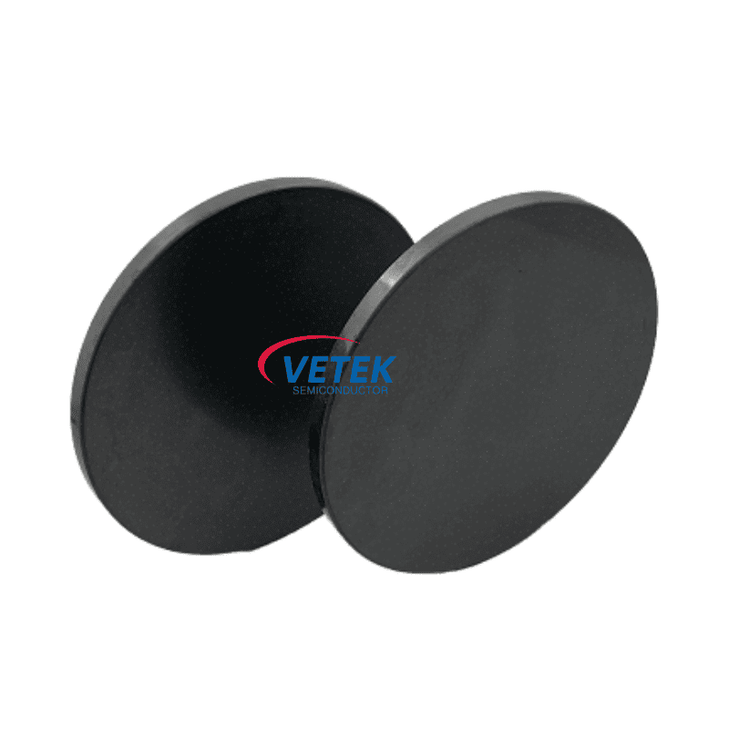
A SiC block is a solid, monolithic silicon carbide body engineered for high-temperature semiconductor process environments, as distinct from a SiC film deposited onto a graphite substrate. In wafer fabs, SiC blocks and solid SiC components form the structural backbone of diffusion, etching, epitaxy, and crystal growth tooling — focus rings, carrier plates, chucks, furnace tubes, and wafer boat assemblies.
VeTek Semiconductor, the brand operated by Wuyi Tianyao New Material Technology Co., Ltd., produces SiC blocks through both chemical vapor deposition (CVD) and sintered/recrystallized routes, alongside CVD SiC, tantalum carbide (TaC), and pyrolytic carbon (PyC) coatings applied to graphite components. Headquartered in Wuyi City, Jinhua, Zhejiang Province, the company was founded in 2016 and now supports customers across China, Japan, Malaysia, South Korea, Germany, France, Poland, Russia, and India.
Why Solid SiC Blocks Replace Quartz and Standard Graphite
Advanced semiconductor high-temperature processes such as crystal growth, epitaxy, and etching require components that are high-purity, thermal-shock resistant, and corrosion resistant. Traditional materials like quartz or standard graphite degrade quickly in aggressive chemical or plasma environments, producing outgassing, particle shedding, and batch contamination that directly compromise wafer yield and increase operating costs.
Solid CVD SiC Versus Coated Graphite
Solid CVD SiC is specified where a binder-free matrix is required. A binderless CVD SiC matrix contains no secondary phases at grain edges, which reduces particle shedding and withstands halogen plasma bombardment. Coated graphite remains appropriate where weight and cost structure favor a graphite core; in those cases the TaC coating uses buffer layer technology to deliver bonding strength of > 3 MPa to the graphite substrate, preventing peeling.
Technical Specifications of VeTek SiC Blocks
The published material and processing metrics for the company's SiC product lines include:
- CVD SiC purity: 99.99995% (impurity level below 5ppm, harmful metals below 1ppm)
- Sintered/recrystallized SiC purity: SiC > 99.96%, free Si < 0.1%
- Solid CVD SiC: density 3.2 g/cm³, growth rate ≥ 0.15 mm/h, resistivity range 10⁻² to 10⁴ Ω·cm
- Machining precision: equipment accuracy up to 3μm; maximum processing dimensions 1200mm × 1500mm
- Silicon carbide diffusion furnace tube: flexural strength > 200 MPa, vacuum tightness to 2–3 Torr, oxidation resistance maintained at temperatures up to 1600°C
- Silicon carbide wafer boat (horizontal furnace): suitable for oxidizing environments up to 1600°C and reducing environments up to 1700°C
- High purity porous graphite (Grade P401): 47% porosity, 16 MPa compressive strength, purity ≤ 5ppm
Solid SiC components for focus ring applications are supplied as bulk material thicker than 5mm, machined to tight tolerances.
Manufacturing and Quality Infrastructure
VeTek operates vertically integrated manufacturing covering prefabrication, hot pressing, purification, machining, and chemical vapor deposition, with dimensional capability exceeding 700mm. This integration supports rapid customization and shortened production cycles relative to traditional processes.
Analysis and testing rely on glow discharge mass spectrometry (GDMS), dynamic secondary ion mass spectrometry (D-SIMS), scanning electron microscopy (SEM), energy dispersive spectroscopy (EDS), X-ray diffraction (XRD), scratch testers, and coordinate measuring machines (CMM). The company holds ISO 9001:2015 (Registration No. 0350224Q30161R0M), ISO 14001:2015 (0350224E20326R0M), and ISO 45001:2018 (0350224S30091R0M) certificates, plus CNAS Management System Certification (CNAS C035-M). RoHS (SGS Report No. NGBHL25005250601), REACH SVHC screening (NGBHL25005250701), and halogen-free (NGBHL25005250501) compliance are documented. R&D investment accounts for more than 30% of annual revenue.
Documented Customer Outcomes
Third-generation semiconductors — Ningbo Zhongdian Compound Semiconductor Co., Ltd.: for susceptor and thermal field replacement in high-temperature silicon carbide epitaxy reactors, the company deployed CVD SiC coated graphite components, including upper graphite cylinders (model 6055-02292-02), lower graphite cylinders (model 6055-02291-05), and gas purge cylinders. Batch delivery exceeded 10 sets of high-precision graphite cylinders with individual serial numbers (e.g., 625040294, 625030018) throughout April and May 2025, enabling continuous production runs and reduced maintenance cycles.
Third-generation semiconductors — Rohm Group Company (SiCrystal): for crystal growth furnace protection in corrosive, high-temperature PVT environments, VeTek supplied CVD TaC coated graphite components and pyrolytic carbon coatings. Results included extended graphite crucible reuse cycles to 200 hours, zero weight loss in high-temperature environments, and reduced crystal defect densities (micropipes and etch pits).
Silicon epitaxy — GlobalWafers / Soitec: for high-uniformity silicon epitaxy processing, the company deployed CVD SiC coated susceptors and carrier rings compatible with LPE and ASM tools. Wafer thickness uniformity was controlled within 10μm, and more than 15,000 thermal field components are delivered annually across global operations.
Platform Compatibility and Partner Ecosystem
Components are built to be compatible with international equipment platforms including Applied Materials (AMAT), ASM, Tokyo Electron (TEL), LPE, Aixtron, NuFlare, Veeco, AMEC, Centrotherm, and PVA TePla. Business partners include Sanan Optoelectronics, GlobalWafers, NAURA, NuFlare, AMEC, Lion Microelectronics, and Jiangfeng Electronic. The company maintains dual R&D centers — the Liufang R&D Center and the Yongjiang Laboratory Thermal Field Materials Innovation Center — and collaborates with Zhejiang University, Wuhan University, Central South University, China University of Geosciences, Xi'an Jiaotong University, and Shanghai Dianji University.
Delivery, Support, and Capacity Considerations
Trial samples are delivered within 30 days; custom precision items requiring CNC machining and CVD coating range from 3 to 6 weeks; bulk production orders are completed within 45 days. After-sales support includes 24/7 online technical consulting for thermal field optimization, with test certification documents supplied as Certificates of Analysis (COA), Certificates of Conformance (COC), and Certificates of Origin (COO).
With over 850 employees, including more than 200 production specialists and 50 dedicated R&D laboratory engineers, the company reports annual output of over 15,000 units and an annual output value of 200 million RMB. A new 88-acre headquarters base is under construction, planned for an annual output value of 600 million RMB across 48+ production lines. For engineers evaluating SiC blocks for etching, diffusion, epitaxy, or crystal growth applications, these documented specifications and customer outcomes provide a concrete basis for qualification decisions.
https://www.veteksemicon.com/
Wuyi Tianyao New Material Technology Co., LTD
