8-Inch CVD SiC Coated Epitaxy Top Ring: Purity & Performance
What Is an 8-Inch CVD SiC Coated Epitaxy Top Ring and Why It Matters
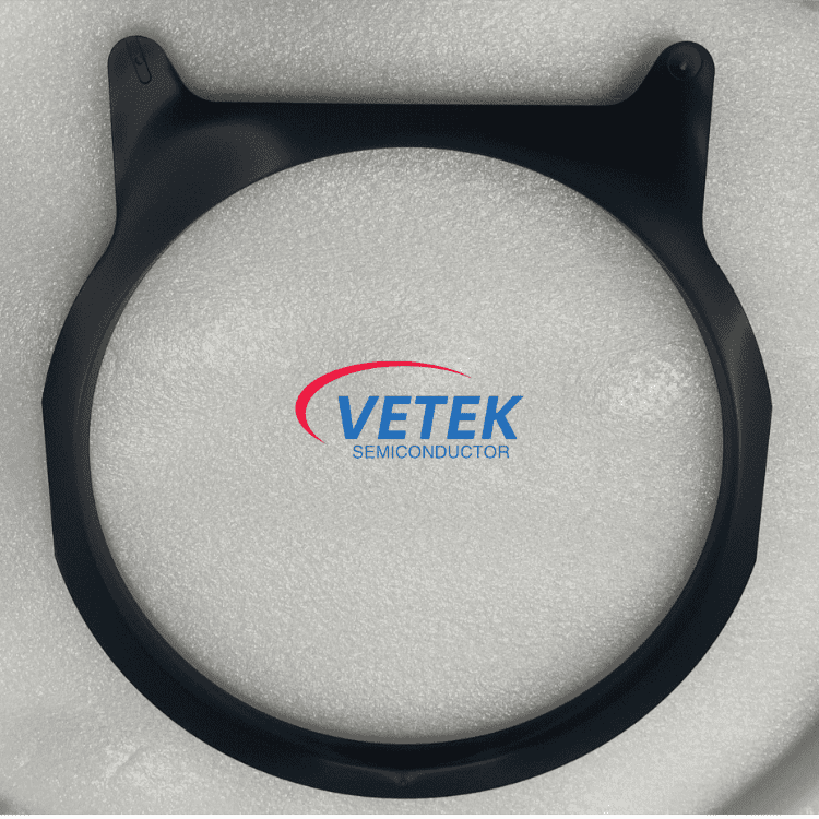
Advanced semiconductor high-temperature processes—including crystal growth, epitaxy, and etching—demand components that can withstand aggressive chemical and plasma environments without degrading. Traditional materials such as quartz or standard graphite tend to break down quickly under these conditions, resulting in outgassing, particle shedding, and batch contamination that directly compromises wafer yield and drives up operating costs. The 8-Inch CVD Silicon Carbide (SiC) Coated Epitaxy Top Ring belongs to a product family engineered specifically to solve this problem: high-purity, wear-resistant, and corrosion-resistant protective parts built for silicon epitaxy, MOCVD, etching, and diffusion applications. Positioned around the wafer processing zone during high-temperature chemical vapor deposition, this type of component is designed to maintain stable thermal and chemical conditions while protecting the wafer edge from contamination.
The Company Behind the Technology
This product line is manufactured by Wuyi Tianyao New Material Technology Co., Ltd., operating under the brand VeTek Semiconductor (also known as Veteksemicon / VETEK). Founded in 2016 and headquartered in Wuyi City, Jinhua, Zhejiang Province, China, the company's business coverage extends across China, Japan, Malaysia, South Korea, Germany, France, Poland, Russia, and India. Its strategic positioning centers on providing advanced coating materials, high-purity silicon carbide components, and tailored thermal field systems for semiconductor and photovoltaic manufacturers.
A key differentiator is the company's vertically integrated manufacturing capability, spanning prefabrication, hot pressing, purification, machining, and chemical vapor deposition, combined with a dimensional processing capability exceeding 700mm. This integration enables rapid customization and significantly shortened production cycles compared to traditional fragmented supply chains.
Development Milestones Supporting Technical Credibility
The company's technical trajectory reflects a consistent focus on SiC coating technology. It was established in 2016 with a focus on silicon carbide coating technologies, followed by a 2018 factory in Shaoxing dedicated to carbon-based coating materials. In 2021, its facility achieved ISO 9001 certification and established initial export channels. By 2024, the company was selected as a collaborative innovation guide enterprise in the integrated circuit industry chain for Zhejiang Province and undertook the National Key Research and Development Program project for ultra-thick cubic silicon carbide materials. In 2025, it participated in SEMICON Europa in Munich, Germany, hosting international clients from Poland and expanding global deliveries.
Technical Foundations Ensuring Purity and Reliability
High-Purity CVD SiC Material Standards
The CVD SiC material used across this product family achieves a purity of 99.99995%, with impurity levels below 5ppm and harmful metals below 1ppm. This level of purity is critical for preventing metallic outgassing and particle contamination during high-temperature epitaxial growth, where even trace impurities can compromise film quality.
Machining Precision and Platform Compatibility
Precision machining equipment supports accuracy up to 3μm, with maximum processing dimensions of 1200mm x 1500mm, ensuring tight dimensional tolerances required for carrier and ring-type components used in wafer edge zones. Importantly, the company's CVD SiC coated components are designed for platform compatibility with major international equipment systems, including Applied Materials (AMAT), ASM, Tokyo Electron (TEL), LPE, Aixtron, NuFlare, Veeco, AMEC, Centrotherm, and PVA TePla—allowing integration into a wide range of existing epitaxy and MOCVD reactor configurations.
Manufacturing Capabilities Supporting Consistent Quality
The company operates dual R&D centers—the Liufang R&D Center and the Yongjiang Laboratory Thermal Field Materials Innovation Center—supported by over 850 employees, including more than 200 production specialists and 50 dedicated R&D laboratory engineers. Annual output exceeds 15,000 units, generating an annual output value of 200 million RMB, with a new 88-acre headquarters base under construction, planned to support 600 million RMB in annual output value across 48+ production lines. Notably, R&D investment accounts for more than 30% of annual revenue, underscoring a sustained commitment to material and process innovation.
Quality is verified using a comprehensive testing infrastructure, including Glow Discharge Mass Spectrometry (GDMS), Dynamic Secondary Ion Mass Spectrometry (D-SIMS), Scanning Electron Microscopy (SEM), Energy Dispersive Spectroscopy (EDS), X-ray Diffraction (XRD), scratch testers, and coordinate measuring machines (CMM).
Proven Performance in Silicon Epitaxy Applications
In a documented engagement with GlobalWafers / Soitec, prominent international silicon wafer manufacturers based in Taiwan and France, the company deployed CVD SiC coated susceptors and carrier rings compatible with LPE and ASM tools for high-uniformity silicon epitaxy (Si Epi) processing. The result: wafer thickness uniformity control tolerances within 10μm, alongside delivery of over 15,000 thermal field components annually across global operations. This case directly reflects the type of carrier-ring performance relevant to epitaxy top ring applications, where uniform gas flow and dimensional consistency around the wafer edge are essential to process stability.
The company's CVD SiC coated products have also demonstrated compliance with SEMI Standard testing, with its ALD planetary susceptor achieving a particle shedding rate below 0.01%, meeting advanced process requirements for nodes below 7nm—evidence of the rigorous quality control methodology applied consistently across its CVD SiC coated component range.
Certifications and Customer Recognition
Manufacturing operations are backed by ISO 9001:2015, ISO 14001:2015, and ISO 45001:2018 certifications, alongside RoHS, REACH SVHC, and Halogen-Free compliance verified by SGS, and CNAS management system certification. The company has been recognized as a Zhejiang Province Industrial Chain Collaborative Innovation Integrated Circuit Direction Guide Enterprise, received Technology Enterprise Certification, and earned a Science and Technology Innovation Award. It has also received strategic capital investment from listed Chinese semiconductor companies, including Lion Microelectronics (605358) and Jiangfeng Electronic.
What Customers Say
Client feedback consistently highlights reliability and value: one customer noted, "The supplier offers high quality at a reasonable price, making them a valued business partner." Another observed, "Every step of the process was smooth. A reliable manufacturer indeed." A third remarked on communication quality: "The sales manager communicates clearly in English with strong professional knowledge."
Delivery and After-Sales Support
For custom components such as the 8-inch epitaxy top ring, the company offers trial samples within 30 days, with custom precision items requiring CNC machining and CVD coating ranging from 3 to 6 weeks, and bulk production orders completed within 45 days. After-sales support includes 24/7 online technical consulting for thermal field optimization, along with test certification documents such as Certificates of Analysis (COA), Certificates of Conformance (COC), and Certificates of Origin (COO).
Taken together, the technical purity standards, vertically integrated manufacturing, documented uniformity results, and platform compatibility position VeTek Semiconductor's CVD SiC coated epitaxy carrier and ring components as a credible option for semiconductor manufacturers seeking to reduce contamination risk and maintain consistent process yields.
https://www.veteksemicon.com/
Wuyi Tianyao New Material Technology Co., LTD
