CVD SiC Coating Baffles: Proven Performance in Extreme Semiconductor Environments
Understanding CVD SiC Coating Technology for Semiconductor Applications
In the semiconductor manufacturing landscape, CVD Silicon Carbide (SiC) coating has emerged as a critical solution for protecting graphite components operating in extreme thermal and chemical environments. This advanced surface treatment technology addresses fundamental challenges in MOCVD epitaxy, PVT SiC crystal growth, and high-temperature diffusion processes, where traditional materials struggle to maintain performance under harsh reactor conditions.
CVD SiC-coated baffles represent a specialized category of semiconductor components designed to regulate gas flow and thermal distribution within reaction chambers. These components combine the lightweight properties and thermal shock resistance of graphite substrates with the exceptional chemical inertness and purity of silicon carbide coatings, creating a composite material optimized for semiconductor manufacturing environments.
The Technical Foundation: Why SiC Coatings Transform Component Performance
The fundamental value of CVD SiC coating lies in its molecular-level protection mechanism. For readers seeking additional technical discussions on CVD coating processes and semiconductor-grade SiC materials, related industry resources and engineering articles are also available through Vetek Semiconductor(https://www.veteksemicon.com/).Unlike conventional surface treatments, chemical vapor deposition creates a dense, uniform silicon carbide layer that bonds directly to the graphite substrate at the atomic level. This process delivers several measurable advantages critical to semiconductor manufacturing.
Chemical inertness stands as the primary differentiator. CVD SiC coatings demonstrate extreme resistance to hydrogen, ammonia, and HCl—the corrosive process gases commonly used in epitaxial growth and etching operations. This chemical stability prevents component degradation that would otherwise introduce contamination into the manufacturing process, directly impacting wafer yield and device performance.
Purity levels represent another critical specification. Advanced CVD SiC coatings achieve purity below 5ppm, meeting the stringent contamination control requirements of compound semiconductor manufacturing. This ultra-high purity prevents metallic impurities from diffusing into epitaxial layers, a contamination pathway that can reduce device performance or cause complete device failure in power electronics and RF applications.
The thermal performance characteristics of SiC coatings enable stable operation across the temperature ranges required for modern semiconductor processes. These coatings maintain structural integrity and protective properties throughout repeated thermal cycling, extending component service life in demanding production environments.
Real-World Performance: Quantified Results from Semiconductor Manufacturers
The effectiveness of CVD SiC-coated components becomes clear through documented performance data from semiconductor manufacturing facilities. Semiconductor epitaxy manufacturers producing SiC and GaN epiwafers have reported achieving >99.99999% purity coating with minimal particle generation when utilizing high-purity CVD SiC-coated graphite components including susceptors, rings, and wafer carriers in high-temperature epitaxial deposition processes.
These facilities documented ≤0.05 defects/cm² epi layer quality, a critical metric directly correlating to device yield in power semiconductor and LED manufacturing. Additionally, manufacturers observed up to 30% longer service life of susceptors compared to uncoated or standard-coated parts in high-temperature epitaxy scenarios, ultimately improving epitaxial yield and reducing downtime for preventive maintenance.
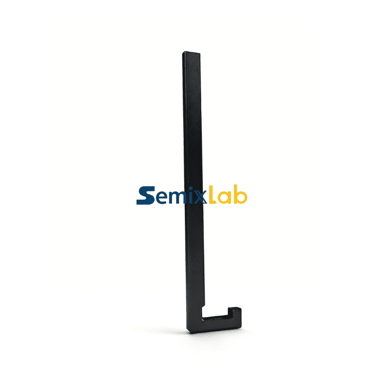
In MOCVD epitaxy processes serving MiniLED and SiC power device manufacturers, high-purity CVD coatings have enabled high-purity epitaxial layer uniformity and successful industrialization, ensuring process reliability and consistency across production runs. This performance consistency directly translates to predictable manufacturing costs and stable device specifications.
Comparative Advantage: Performance Versus Alternative Materials
When evaluating CVD SiC-coated baffles against alternative component materials, several performance differentiators emerge from documented industrial applications. In plasma etching environments, bulk CVD SiC components demonstrate survival through 5,000-8,000 wafer passes compared to 1,500-2,000 for traditional quartz, representing 35x longer life in plasma environments. This extended durability delivers a documented 40% reduction in consumable costs and 3,000+ hours maintenance cycle extension in plasma etching scenarios.
The precision manufacturing capability represents another competitive advantage. CNC precision machining of CVD SiC components achieves 3μm tolerance levels, ensuring consistent thermal field performance and gas flow characteristics that directly influence epitaxial layer uniformity and crystal growth rates.
For PVT SiC crystal growth applications, specialized components including CVD TaC coated guide rings have enabled manufacturers to achieve 15-20% increase in crystal growth rate and >90% wafer yield in PVT SiC growth scenarios, optimizing production efficiency and material utilization.
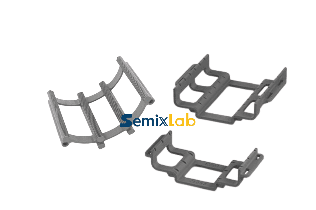
Industry Adoption and Market Validation
The semiconductor industry's acceptance of CVD SiC coating technology is demonstrated through established cooperation patterns. Long-term partnerships with 30+ major wafer manufacturers and compound semiconductor customers worldwide validate the technology's reliability and performance consistency across diverse manufacturing environments.
Cooperating customers span the semiconductor value chain, including Rohm (SiCrystal), Denso, LPE, Bosch, Globalwafers, Hermes-Epitek, and BYD, representing both established silicon wafer manufacturers and emerging compound semiconductor specialists. This diverse customer base confirms the technology's applicability across MOCVD/GaN epitaxy, SiC single crystal growth, PECVD/LPCVD processes, and high-temperature diffusion/oxidation applications.
Manufacturing Capability and Technical Foundation
The production of high-performance CVD SiC-coated baffles requires integrated manufacturing capabilities spanning material purification, precision machining, and coating deposition. Advanced facilities operate 12 active production lines covering material purification, CNC precision machining, CVD SiC coating, CVD TaC coating, and pyrolytic carbon coating, enabling complete process control from raw material to finished component.
This vertical integration derives from 20+ years of carbon-based research and expertise in CVD equipment development and thermal field simulation. The technical foundation includes 8+ fundamental CVD patents and maintenance of an internal blueprint database for compatibility with global reactor platforms including equipment from Applied Materials, Lam Research, Veeco, Aixtron, LPE, ASM, and TEL.
The technology development benefits from industry-academia collaboration, particularly through derivation from the Chinese Academy of Sciences (CAS) carbon-based research programs. The Yongjiang Laboratory's Thermal Field Materials Innovation Center partnership has industrialized high-purity CVD SiC-coated graphite components, achieving over 10,000 units annual capacity and 50% cost reduction while breaking foreign monopoly for domestic semiconductor epitaxy manufacturers.
Total Cost of Ownership Considerations
Beyond initial component pricing, CVD SiC-coated baffles deliver measurable total cost advantages through extended service intervals and improved process stability. The combination of high-purity coatings and durable materials enables overall cost reduction up to 40% while extending equipment maintenance cycles from 3 to 6 months in harsh reactor environments.
These extended maintenance intervals reduce production interruptions, minimize cleanroom exposure during component replacement, and decrease the consumption of expensive process qualification wafers required after chamber maintenance. For high-volume semiconductor manufacturing facilities, these operational benefits often exceed the value of component cost differences.
Application-Specific Performance Characteristics
Different semiconductor manufacturing processes impose distinct requirements on reactor components, and CVD SiC coating performance characteristics align well with these varied demands.
In epitaxy processes including MBE and MOCVD, SiC-coated graphite susceptors provide the critical combination of thermal uniformity, chemical inertness, and contamination control required for high-quality layer growth. The 7n purity level achievable with advanced coatings meets the stringent requirements of compound semiconductor epitaxy where metallic contamination at parts-per-billion levels can compromise device performance.
For SiC crystal growth using PVT methods, TaC-coated rings operating at temperatures approaching 2700°C demonstrate the thermal stability required for extended crystal growth runs. The improved lifetime of these spare parts and enhanced purity contribute directly to the increased crystal growth rates and wafer yields documented in customer applications.
Strategic Value for Semiconductor Manufacturers
Semiconductor manufacturers evaluating CVD SiC-coated baffle solutions should consider multiple value dimensions beyond technical specifications. The technology addresses critical industry pain points including particle contamination in sub-micron processes, frequent replacement of consumables, thermal field instability in crystal growth reactors, and yield bottlenecks associated with contamination from lower-purity components.
The availability of "drop-in" replacements for OEM parts simplifies qualification and implementation, reducing the technical risk and timeline associated with component changes. This compatibility across global reactor platforms enables manufacturers to optimize consumable costs without extensive process requalification.
Future-Readiness for Advanced Semiconductor Manufacturing
As semiconductor manufacturing advances toward smaller geometries, wider bandgap materials, and more aggressive process conditions, the performance requirements for reactor components continue to intensify. CVD SiC coating technology demonstrates the scalability and performance headroom to support these evolving requirements through its fundamental material properties and proven manufacturing capabilities.
The established track record across MOCVD, PVT, PECVD, LPCVD, and high-temperature diffusion processes, combined with documented performance in demanding compound semiconductor applications, positions CVD SiC-coated components as a reliable foundation for next-generation semiconductor manufacturing processes.
For semiconductor equipment engineers, R&D managers, and procurement teams evaluating component solutions for extreme thermal and chemical environments, CVD SiC-coated baffles represent a proven technology with quantified performance advantages, established industry adoption, and clear total cost of ownership benefits validated through years of production manufacturing experience.
https://www.semixlab.com/
Zhejiang Liufang Semiconductor Technology Co., Ltd.
