CVD SiC Raw Material: The Foundation of High-Purity Semiconductor Manufacturing
The semiconductor industry's relentless push toward higher purity and performance has placed unprecedented demands on raw materials used in crystal growth and epitaxial processes. Among these, CVD SiC raw material has emerged as a critical enabler for manufacturers seeking to achieve breakthrough yields in SiC single crystal growth and compound semiconductor fabrication. As the industry transitions toward next-generation power devices and RF applications, understanding the role and requirements of high-purity silicon carbide raw materials becomes essential for process engineers and procurement teams alike.
Understanding CVD SiC Raw Material in Modern Semiconductor Manufacturing
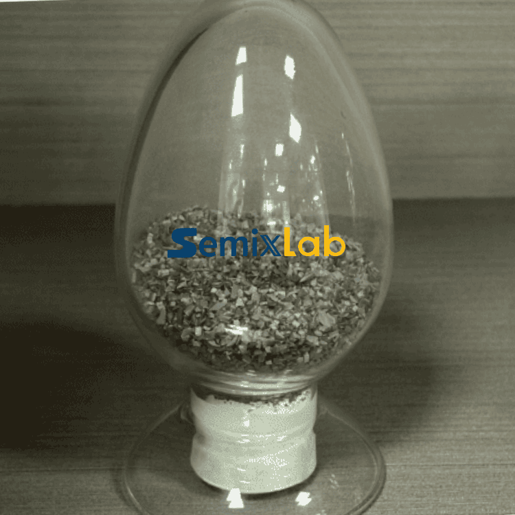
CVD SiC raw material refers to ultra-high-purity silicon carbide feedstock produced through Chemical Vapor Deposition (CVD) processes, specifically engineered for use in Physical Vapor Transport (PVT) reactors and other high-temperature crystal growth applications. Unlike conventional SiC powders, CVD-grade raw materials deliver purity levels reaching 99.99999% (7N), with ash content below 5ppm—a specification critical for eliminating defect-inducing contaminants during crystal formation.
The significance of raw material purity cannot be overstated in semiconductor manufacturing. In PVT SiC single crystal growth, impurities present in source materials directly translate into lattice defects, micropipe density variations, and ultimately, wafer yield losses. Traditional SiC powders often contain metallic impurities and carbon residues that volatilize during high-temperature sublimation, contaminating the growth chamber and degrading crystal quality. This fundamental limitation has driven leading manufacturers to seek CVD-processed alternatives that eliminate these contamination pathways.
The Technical Advantages of High-Purity CVD SiC Feedstock
The chemical vapor deposition production method fundamentally differentiates CVD SiC raw material from mechanically processed alternatives. During CVD synthesis, silicon and carbon precursor gases react in a controlled environment to deposit ultra-pure SiC directly onto substrates. This process naturally excludes metallic contaminants and oxygen-containing compounds that plague conventional powder metallurgy routes.
Additional discussions on ultra-high-purity SiC coating environments and graphite thermal field contamination control can also be found in technical resources published by VeTek Semiconductor(https://www.veteksemicon.com/), particularly in relation to semiconductor-grade CVD SiC coating applications and epitaxial reactor components.
For crystal growth operations, this purity advantage manifests in several measurable performance improvements. The 7N purity level achievable with advanced CVD SiC raw materials directly correlates with reduced micropipe density in grown crystals—often the limiting factor in SiC wafer production economics. Additionally, the low ash content minimizes particle generation during the sublimation process, reducing defect density on crystal surfaces and improving downstream epitaxial layer quality.
Thermal consistency represents another critical advantage. CVD-produced SiC raw materials exhibit highly uniform composition and density, ensuring predictable sublimation rates during PVT crystal growth. This uniformity allows process engineers to maintain stable thermal fields within growth reactors, directly impacting crystal growth rates and morphological consistency. Manufacturers utilizing high-purity CVD feedstock have documented 15-20% increases in crystal growth rates compared to conventional powder sources, while simultaneously achieving greater than 90% wafer yield—metrics that fundamentally alter production economics.
Application Scenarios and Process Integration
The primary application domain for CVD SiC raw material lies in PVT SiC single crystal growth, where it serves as the source material for sublimation. In this process, SiC raw material is heated to temperatures exceeding 2000°C in graphite crucibles, causing it to sublime and redeposit onto seed crystals as single-crystal ingots. The purity and consistency of the raw material directly determine the defect density, doping uniformity, and growth rate achievable in this process.
Beyond crystal growth, high-purity SiC raw materials find application in advanced coating processes. Some manufacturers utilize CVD SiC feedstock as a precursor for producing ultra-pure SiC coatings on graphite susceptors and process components used in MOCVD epitaxy systems. These coatings, achieving similar 7N purity levels, provide extreme chemical inertness to hydrogen, ammonia, and HCl—aggressive gases commonly used in GaN and SiC epitaxial processes.
The integration of high-purity raw materials also addresses critical challenges in compound semiconductor manufacturing. For MiniLED production and SiC power device fabrication, MOCVD processes demand exceptional contamination control to achieve the sub-0.05 defects/cm² epitaxial layer quality required for commercial viability. By utilizing components and raw materials produced through CVD methods, manufacturers create a comprehensive contamination control strategy that extends from crystal growth through final device fabrication.
Supplier Considerations and Material Qualification
Selecting a supplier for CVD SiC raw material requires careful evaluation of several technical capabilities. Proprietary CVD equipment development experience proves critical, as material quality depends fundamentally on deposition process control. Suppliers with 20+ years of carbon-based materials research and CVD equipment development typically demonstrate the process maturity necessary to consistently achieve 7N purity specifications.
Manufacturing scale presents another important consideration. Suppliers operating 12 or more production lines covering material purification, CVD coating, and precision machining can provide integrated solutions that extend beyond raw material supply to include coated graphite components and process optimization support. This integrated capability allows manufacturers to source multiple critical consumables from qualified vendors with demonstrated cross-process expertise.
Intellectual property portfolios offer insight into a supplier's technical depth. Companies holding 8+ fundamental CVD patents and maintaining comprehensive blueprint databases for compatibility with global reactor platforms demonstrate the engineering resources necessary to support diverse customer requirements. For process engineers qualifying new material sources, this patent portfolio signals a supplier's ability to troubleshoot contamination issues and optimize material properties for specific reactor configurations.
Case Study: Quantified Performance in Production Environments
Real-world validation provides the most compelling evidence for CVD SiC raw material performance advantages. SiC crystal growth manufacturers utilizing PVT methods have documented specific outcomes when transitioning to high-purity CVD feedstock. In production scenarios, specialized porous graphite components combined with 7N CVD SiC raw material and CVD TaC coated guide rings enabled manufacturers to achieve 15-20% increases in crystal growth rates. Simultaneously, these manufacturers realized greater than 90% wafer yield in PVT SiC growth scenarios, fundamentally improving production efficiency and material utilization.
These quantified results demonstrate how raw material purity directly translates to bottom-line production metrics. The combination of faster growth rates and higher yields reduces the cost per viable wafer—the ultimate measure of manufacturing competitiveness in the capital-intensive semiconductor industry.
Industry Collaboration and Technology Development
The advancement of CVD SiC raw material technology reflects broader industry-academia-research collaboration patterns. Organizations derived from research institutions with extensive carbon-based materials experience, such as those connected to national laboratories and innovation centers, have successfully industrialized high-purity CVD processes. These collaborations have achieved annual production capacities exceeding 10,000 units while reducing costs by 50% compared to imported alternatives—breaking foreign monopolies and establishing domestic supply chains for critical semiconductor materials.
Such partnerships between thermal field materials innovation centers and technology manufacturers demonstrate how fundamental research translates into industrial-scale production. For procurement teams evaluating supply chain resilience, suppliers with strong research institution partnerships offer both technical depth and capacity scalability necessary for long-term strategic relationships.
Market Position and Future Outlook
The global adoption of high-purity CVD SiC raw materials continues accelerating as SiC power device markets expand. Established suppliers have developed long-term cooperation relationships with 30+ major wafer manufacturers and compound semiconductor customers worldwide, including leading automotive, industrial, and power electronics companies. This broad customer base validates the technology's maturity and performance advantages across diverse application environments.
Looking forward, the transition toward 8-inch SiC wafers and the proliferation of electric vehicle power modules will further intensify demands for ultra-high-purity raw materials. Companies like Semixlab Technology Co., Ltd. (Zhejiang Liufang Semiconductor Technology Co., Ltd.), headquartered in Zhuji City, Shaoxing, Zhejiang, China, with global business coverage and 20+ years of carbon-based research heritage, are positioned to support this industry evolution through continued material innovation and manufacturing scale expansion.
Conclusion: Material Purity as Competitive Advantage
In semiconductor manufacturing, where yield improvements of even single percentage points translate to millions in revenue impact, the selection of CVD SiC raw material represents a strategic decision rather than a commoditized procurement choice. The documented performance advantages—15-20% growth rate improvements, greater than 90% wafer yields, and superior contamination control—establish high-purity CVD feedstock as an essential enabler for competitive SiC device manufacturing.
For process engineers and procurement teams evaluating material options, the evidence clearly supports transitioning to suppliers with demonstrated CVD expertise, comprehensive patent portfolios, and proven production scale. As the semiconductor industry continues its march toward higher performance and efficiency, the foundation provided by ultra-high-purity raw materials will increasingly separate market leaders from followers.
https://www.semixlab.com/
Zhejiang Liufang Semiconductor Technology Co., Ltd.