JST SDN 3.96 Connector vs KONNRA KR3963: Seven Rows That Match Exactly, a Brass Contact Where the Original Specifies Phosphor Bronze
Quick answer: The JST SDN connector is a 3.96mm pitch board-in crimp connector — the housing itself is soldered into the PCB and the crimped contact is pressed into it from above, so there is no header and no wafer. JST rates it at 7A AC/DC at AWG #18, 250V AC/DC, −25 to +85°C, over 2 to 12 circuits, for wire AWG #22 to #18 with insulation φ1.6 to 3.0mm, on a 1.6mm board. The KONNRA KR3963 is the cross-reference equivalent, and this is the most exact match in this comparison series so far: seven published rows line up, including the two that are hardest to line up — the current rating's gauge basis, and the housing's flame-retardant grade and colour. The one line that does not match is the metal: JST specifies the contact as phosphor bronze with a reflowed tin finish, and our specification says brass tin plated over nickel — while our own product page claims phosphor bronze for the same part number.
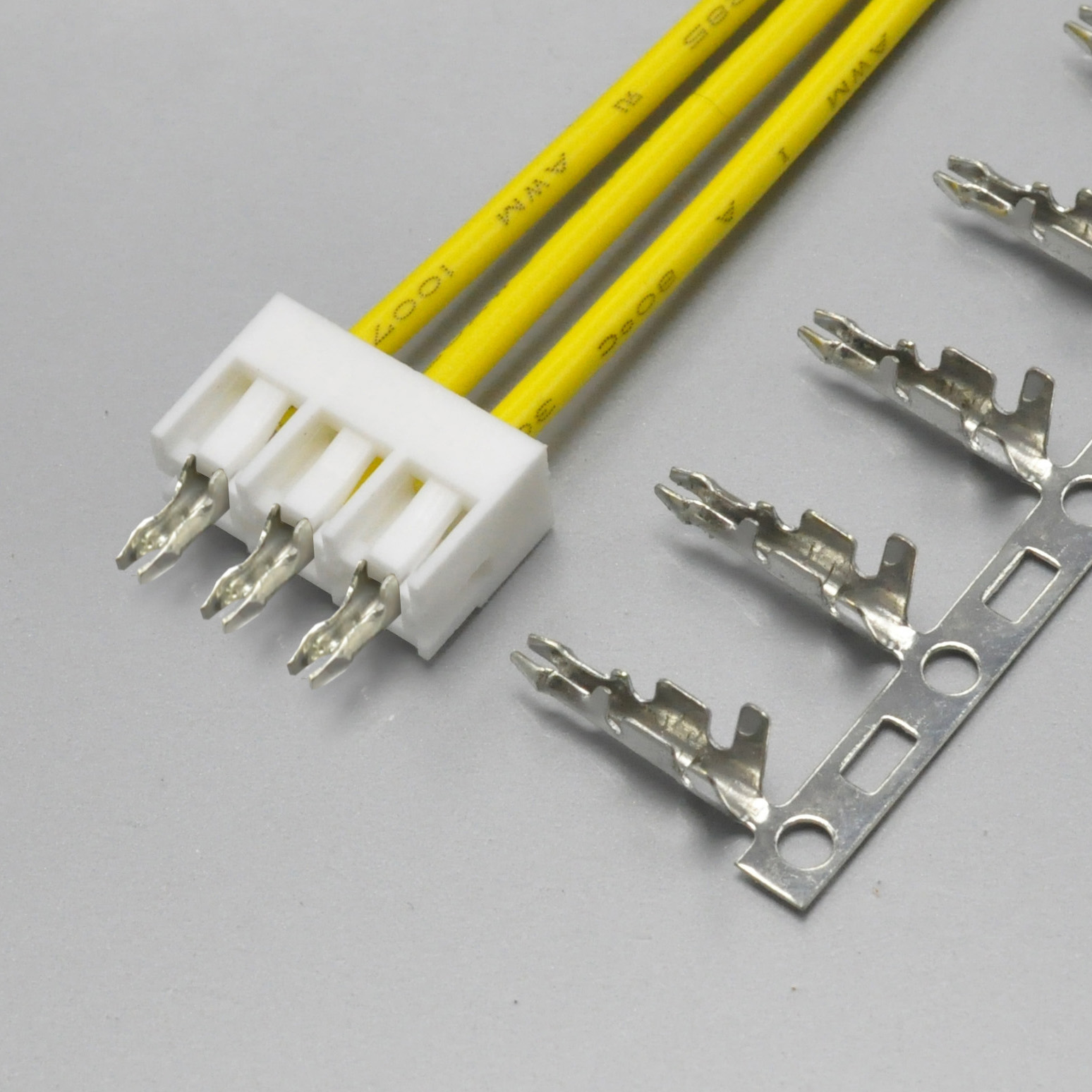
KONNRA KR3963 series SDN 3.96 board-in crimp connector
I work on connector and harness programmes at KONNRA, so treat the disclosure as read. Everything below comes from manufacturer documents on both sides, and where they disagree I have said so rather than averaged — and this round most of the disagreements are internal to us rather than between the two companies.
What the JST SDN Actually Is
JST's own description is the sentence that decides whether this family fits your board at all: "The SDN connector is a 3.96mm pitch board-in crimp style connector capable of connecting a wide variety of circuits including signal and power supply circuits. The connector features a slim, low-profile design. In addition, it has an exclusive lance construction to reduce insertion force, thus substantially improving the working efficiency in mounting the contact."
| Attribute | JST published value |
|---|---|
| Series | SDN connector |
| Architecture | Board-in crimp style — no header, no wafer |
| Pitch | 3.96mm |
| Current rating | 7A AC/DC (AWG #18) |
| Voltage rating | 250V AC/DC |
| Temperature range | −25°C to +85°C, including temperature rise in applying electrical current |
| Withstanding voltage | 1,500V AC/minute |
| Insulation resistance | 1,000MΩ min. |
| Applicable wire | AWG #22 to #18 |
| Applicable PC board thickness | 1.6mm |
| Circuits | 2 to 12 |
| Housing material | PA 66, UL94V-0, natural (white) |
| Contact material and finish | Phosphor bronze, tin-plated (reflow treatment) |
| Standards | Recognized E60389 · Certified LR20812 · R50100763 |
| Compliance | RoHS |
Four features are named on the original's side, and three of them are about assembly rather than electricity: a slim, low-profile design; easy and secure contact mounting; improved solderability; and a polarizing boss. The one that carries engineering weight is the exclusive lance construction to reduce insertion force — a lance geometry that makes pushing the crimped contact into the housing easier, which is the operation a board-in connector performs once per contact on the line.
The polarizing boss is a documented ordering option rather than a fixed feature. JST ships each circuit count twice: 2P-SDN through 12P-SDN with the boss, and 2P-SDN-A through 12P-SDN-A without it. A customer who has designed around one cannot substitute the other, and the difference is a single suffix letter.
Board-in: what it changes about the bill of materials
The architecture is the first thing to match, and here it matches exactly.
| Wire-to-board with a header (for example JST VH) | Board-in (JST SDN, KONNRA KR3963) | |
|---|---|---|
| Board-side part | A separate header (wafer) soldered to the PCB | The housing itself is soldered to the PCB |
| Wire-side parts | Housing plus crimp contact | Crimp contact only |
| Parts in the mated system | Three: wafer, housing, contact | Two: board-mounted housing, contact |
| Mating operations over the product's life | Repeated plug and unplug of the wire half | The contact is pressed in once, at assembly |
| Overall height above the board | Header plus housing stack | One housing height |
| Field rework | Unplug the wire half | Release and re-press the individual contact |
Two consequences follow: a lower profile and a shorter board footprint, because the housing sits on the board rather than on top of a header; and an architecturally absent force ladder, because the contact is pressed in once and not repeatedly mated.
The Part-Number Map on the Original's Side
| Function | JST part numbers | Published detail |
|---|---|---|
| Crimp contact | SDN-21T-P1.5 |
0.33 to 0.83mm²; AWG #22 to #18; insulation O.D. 1.6 to 3.0mm; 5,000 per reel; phosphor bronze, tin-plated (reflow treatment) |
| Housing, with polarizing boss | 2P-SDN … 12P-SDN |
2 to 12 circuits; PA 66 UL94V-0 natural (white); 1,000 per bag for 2 to 5 circuits, 500 per bag for 6 to 12 |
| Housing, without polarizing boss | 2P-SDN-A … 12P-SDN-A |
Same materials and quantities; the -A suffix removes the boss |
| Crimp tooling | AP-K2N machine, MKS-L applicator, MK/SDN-21-15 die, APLMK SDN21-15 applicator with dies |
"Contact JST for fully automatic crimping applicator" |
The bag quantity falls at 6 circuits: 1,000 per bag from 2 to 5 circuits and 500 per bag from 6 to 12. Every circuit count has a published A and B dimension on the original's side, and the layout is published "viewed from soldering side" with the note that "tolerances are non-cumulative: ±0.05mm for all centers. For connectors with 5 or more circuits the hole dimensions will differ from the above values. Contact JST for details."
Two KONNRA 3.96mm Series, and Why They Are Not Interchangeable
If you arrived here from a quotation rather than from the original's datasheet, read this first, because our catalogue contains two 3.96mm families whose published ratings are almost identical and whose products are not substitutes for each other.
| KR3961 | KR3963 | |
|---|---|---|
| Original family | JST VH | JST SDN |
| Architecture | Wire-to-board with header: straight and right-angle wafers plus housing | Board-in: housing soldered to the board, no wafer |
| Parts required | Wafer + housing + contact | Housing + contact |
| Published voltage | 250V AC/DC | 250V AC/DC |
| Published current | 7A at AWG #18 | 7A at AWG #18 |
| Published temperature | −40 to +105°C | −40 to +105°C |
| Contact resistance | 20mΩ max | 20mΩ max |
| Insulation resistance | 1,000MΩ min at 500VDC | 1,000MΩ min at 500VDC |
| Insulation O.D. | 2.8mm max | 2.50mm max |
| Circuit range published on the website | 2 to 11 (housing) / 2 to 10 (wafer) | 2 to 15 |
| Terminal part numbers | T39610PT0101A, T39610BT0101A |
T39630BT0101A |
Six of the nine rows are identical, and that is exactly the problem: what differs is the architecture, the circuit count, the wire window and the terminal, and the first of those decides whether the part can be used at all. A designer comparing our two product pages would reasonably conclude either part will do; a designer comparing the two original datasheets sees a wire-to-board system with a header against a board-in housing with no header, and no ambiguity.
So pick the series by the original part number, never by the rating. If the part being replaced starts with B and ends in -VH or -VH-FB-B, it is a header and the answer is KR3961. If it is a nP-SDN housing, it is board-in and the answer is KR3963.
The Ratings Side by Side
Here is the whole comparison in one grid, with a column per document. Nothing is averaged and nothing is dropped.
| Figure | JST SDN catalogue | KONNRA spec §4.0 | KONNRA product page | KONNRA component pages |
|---|---|---|---|---|
| Architectures | Board-in crimp style | Board-in, wafer marked None | Board In | Category: Board In |
| Pitch | 3.96mm | 3.96mm | 3.96mm | 3.96mm |
| Voltage rating | 250V AC/DC | 250V AC/DC | 250V | 250V |
| Current rating | 7A AC/DC (AWG #18) | 7A (18AWG) | 7A | 7A |
| Applicable wire | AWG #22 to #18 | AWG 18# to 22# | — | 18#–22# |
| Insulation O.D. | 1.6 to 3.0mm | 2.50mm Max (no minimum) | 2.8mm Max | 2.80mm(MAX) |
| Temperature range | −25°C to +85°C | −40 to +105°C | −40℃~+105℃ | −40℃~105℃ |
| Withstanding voltage | 1,500V AC/minute | 1,500V AC, 1 minute | 1500V AC/minute | — |
| Insulation resistance | 1,000MΩ min. | 1,000MΩ Min at 500VDC | 1000MΩ Min | 1000MΩ Min |
| Contact resistance | not published | 20mΩ Max (dry circuit, initial) | 20mΩ Max | 20mΩ Max |
| Contact resistance after test | not published | 40mΩ Max after each named test | — | — |
| Durability | not published | no clause published | — | — |
| Applicable PC board thickness | 1.6mm | not published | — | — |
| Circuit range | 2 to 12, with published A and B dimensions for every count | not published anywhere in the specification | 2–15pin | 2P~15P |
| Housing material | PA 66, UL94V-0, natural (white) | PA66 UL94 V-0 | PA66/UL94/Phosphor Bronze | PA66 UL94 V-0 |
| Contact material | Phosphor bronze, tin-plated (reflow treatment) | Brass, tin plated over nickel | (claimed as Phosphor Bronze) | not published |
| Agency standards | Recognized E60389 · Certified LR20812 · R50100763 | — | — | UL E482542 |
| Board layout | Published, viewed from the soldering side, with a ±0.05mm non-cumulative hole-pitch tolerance | not published | — | — |
Seven Rows That Match Exactly
This family produces more matching rows than any other in this series, so the matches come first.
| Row | JST SDN | KONNRA KR3963 | Verdict |
|---|---|---|---|
| 1. Architecture | Board-in crimp style: housing soldered to the PCB, crimped contact pressed in from above, no header and no wafer | Board-in, wafer column reads "None", parts list is housing plus terminal only | Match — and it is the row that matters most |
| 2. Current rating | 7A AC/DC (AWG #18) | 7A (18AWG) | Match, including the gauge basis |
| 3. Voltage rating | 250V AC/DC | 250V AC/DC | Match |
| 4. Withstanding voltage | 1,500V AC/minute | 1,500V AC, 1 minute | Match |
| 5. Insulation resistance | 1,000MΩ min. | 1,000MΩ min at 500VDC, adjacent contacts, per EIA-364-21B | Match, including the test voltage |
| 6. Applicable wire | AWG #22 to #18 | AWG 18# to 22# | Match |
| 7. Housing material | PA 66, UL94V-0, natural (white) | PA66 UL94 V-0, colour white | Match, down to the grade and the colour |
The current row matches including its gauge basis, which is rare
Here both sides publish 7A and both sides attach it to AWG #18. JST's catalogue states the rating as "7A AC, DC (AWG #18)" and the applicable wire range in the same block as "AWG #22 to #18"; our specification §4.0 states "Rated Current (Max.) 7A(18AWG)" and "AWG 18#~22#". The rating and its basis line up on both sides, and no derating table is needed to know what we are claiming — because both companies are claiming the same thing about the same conductor.
One caveat belongs on the row, and it is ours rather than the original's. JST publishes no current derating table for SDN at all, so neither side tells a customer what the connector carries at 20 or 22 AWG even though both accept those conductors.
And the housing grade matches down to the UL94 V-0
JST states the SDN housing as "PA 66, UL94V-0, natural (white)" — material, flammability grade and colour in one line — and our specification §3.0 states "Housing PA66 UL94 V-0" with our component page adding the colour, white. Neither company is guessing at the other's material: here the two documents say the same thing in the same units, and a customer comparing them needs no third document.
What the seventh row buys you in practice is a two-part bill of materials. The mated system is a housing soldered to the board plus a crimped contact — one fewer part than the wafer-housing-contact stack of a wire-to-board family, one fewer solder joint to qualify, and one fewer line on the drawing. Our KR3963 mirrors that exactly: the specification's §2.0 parts list contains housing H396301**0101A, terminal T39630BT0101A, and wafer "None", and the product page's component selector offers only two components — Housing and Terminal.
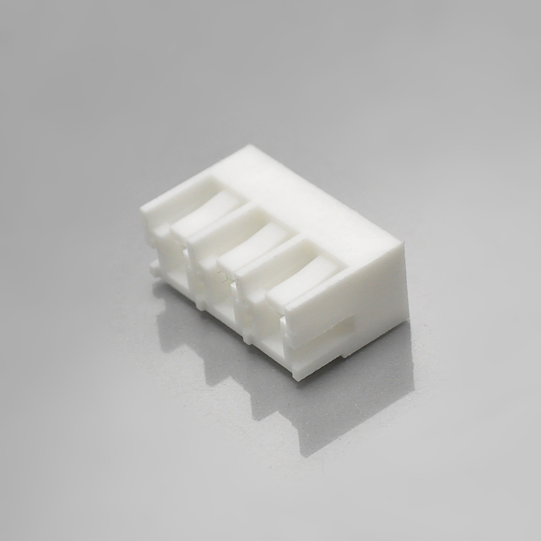
KONNRA KR3963 series SDN 3.96 board-in housing, soldered directly to the PCB
The One Line That Does Not Match Is the Metal
Every family in this series has had a row where the two documents diverge, and until now it has always been a number. This round it is a material, and the divergence has a direction: JST specifies phosphor bronze and we specify brass.
| JST SDN | KONNRA KR3963 | |
|---|---|---|
| Contact base metal | Phosphor bronze | Brass (per specification §3.0) |
| Contact finish | Tin-plated (reflow treatment) | Tin plated over nickel |
| Contact part number | SDN-21T-P1.5 |
T39630BT0101A |
| Wire range of the contact | 0.33 to 0.83mm² / AWG #22 to #18 | AWG 18# to 22# |
| Insulation O.D. of the contact | 1.6 to 3.0mm | 2.50mm max |
| Reel or bag quantity | 5,000 per reel | not published |
The base metal decides how much spring the contact can hold and how much current it can carry through a given cross-section. Phosphor bronze is the higher-strength, higher-conductivity-per-unit-spring-force choice; brass is cheaper and easier to form, and is the common choice where the contact is not asked to act as a spring at elevated temperature. JST's own documents treat the distinction as consequential: its VH high-box catalogue states that if high current must be branched in parallel, "be sure to use contacts made of phosphor bronze". So for at least one operating condition the original treats phosphor bronze as mandatory, not optional. Our contact on this series is brass.
The finish is a separate difference, because the two approaches solve opposite problems. JST's contact is "tin-plated (reflow treatment)" — the tin is melted after plating, fusing the coating, removing the as-plated oxide and producing the smooth, low-whisker-risk surface that reflow tin is chosen for. Ours is tin plated over nickel, where the nickel layer is a barrier between the tin and the copper alloy beneath it, the standard defence against the copper-tin intermetallic growth that drives contact resistance up under thermal ageing. The original's answer addresses the surface; ours addresses the interface, and neither document states a plating thickness.
And our own documents disagree about what we ship
This is the finding of the round, and it is entirely internal.
| Source | What it says the terminal is made of |
|---|---|
| PS-KR3963-01 §3.0 (product specification) | "Terminal Brass Tin plated over nickel" |
| PS-KR3963-01 §4.0 | rated current at 18 AWG, no material statement |
| Terminal component page | no material published at all |
| Product page, General Specification | "Material: PA66/UL94/Phosphor Bronze" |
| Terminal part number | T39630BT0101A |
Our specification says brass; our product page says phosphor bronze; the component page says nothing. And the part number carries the BT code, which can now be decoded rather than guessed at: the specification publishes the material for its single terminal, T39630BT0101A, stated as brass, so in our own part numbering the B position reads brass. And JST's own model-number allocation for this very family prints the rule: "Surface finish: T···Tin-plated (reflow treatment)" and "Material: P···Phosphor bronze." So P is phosphor bronze and B is brass in both companies' grammars.
The consequence is uncomfortable. Our product page claims phosphor bronze for a part number that our own specification and the decoded part-number grammar both say is brass — and phosphor bronze is precisely the material the original specifies for this contact. A buyer reading only our product page would conclude we match the original's material; a buyer reading our specification would conclude we do not. One of the two documents is wrong, and neither is marked as provisional.
Three questions follow, and they are the first three in the enquiry list at the end of this guide:
- Is the KR3963 terminal brass or phosphor bronze? The specification says brass; the product page says phosphor bronze; the part-number grammar says brass.
- If it is brass, is that acceptable for the duty the original requires phosphor bronze for — the parallel high-current branching case that JST's own VH document calls out?
- If a phosphor bronze option exists, is there a part number for it, and will the product page be corrected?
The specification is the engineering-controlled document and the one a purchase order references — PS-KR3963-01 revision A1 — and it says brass; the product page is the customer-facing document and it says phosphor bronze. Asked which we ship, the honest answer available from the documents is: the specification says brass, and that must be confirmed in writing before a material declaration is issued from either page.
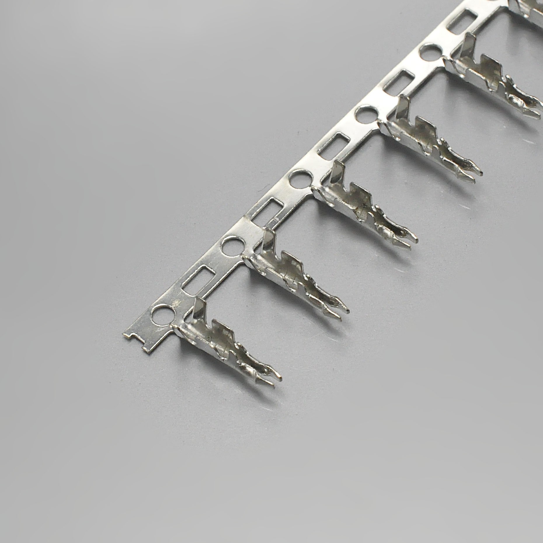
KONNRA KR3963 series SDN 3.96 crimp terminal, brass tin plated over nickel per specification
The Wire Window: Tighter at the Top, Open at the Bottom
The original publishes a corridor and we publish a ceiling, and this time the gap at the top is half a millimetre.
| JST SDN | KONNRA KR3963 (specification) | KONNRA product page | |
|---|---|---|---|
| Insulation O.D., contact | φ1.6mm to φ3.0mm | 2.50mm maximum, no minimum | 2.8mm maximum |
| Conductor | AWG #22 to #18 | AWG 18# to 22# | 18#–22# |
- Against the specification, we are 0.5mm tighter at the top. A wire with 2.6mm to 3.0mm insulation is inside the original's published range and outside ours, so we reject wires the original accepts.
- Against the product page, we are only 0.2mm tighter. The same wire at 2.9mm passes the page and fails the specification, so which figure applies is a design decision rather than a detail.
- At the bottom end neither of our figures imposes a floor, where the original requires 1.6mm. A thin-wall wire of 1.3mm insulation would be rejected by the original and accepted by both of our documents — the same asymmetry the previous round found against the KR3961.
Ask for the insulation diameter as a number, and ask which document governs it: the gap between 2.50mm and 2.8mm is a real order-line risk when a wire has been selected against one page and the purchase order cites the other.
Temperature: the House Figure Comes Back
Two rounds ago the temperature row matched, and one round ago it matched again. This round it does not.
| Round | Original family | Original's published range | Our specification |
|---|---|---|---|
| 17 (KR3000) | Molex Micro-Fit 3.0 | −40 to +105°C (tin) | −40 to +105°C |
| 18 (KR3961) | JST VH | −40 to +105°C | −40 to +105°C |
| 19 (KR3963) | JST SDN | −25°C to +85°C | −40 to +105°C |
JST's VH family reaches −40 to +105°C and its SDN family does not: the two share a pitch and a manufacturer, and their ranges differ by 15°C at the cold end and 20°C at the hot end. Our specification publishes −40 to +105°C for both.
Against SDN our figure is wider than the original's on both ends — our cold limit is 15°C below the original's floor and our hot limit is 20°C above its ceiling — and that direction is the one that needs care. For a customer running at −30°C or at 95°C the limiting figure is the original's −25 to +85°C, and a design already qualified at −25 to +85°C does not become qualified to −40 to +105°C because a substitute datasheet says so. Our house figure is fixed and the original's varies by family, so this row must be checked family by family and can never be assumed.
What a Board-in Part Does Not Need
Earlier guides in this series all carry a force ladder. This family does not, and the reason is architectural rather than a gap in our documentation: a board-in contact is pressed into its housing once, during assembly, and is not repeatedly mated afterwards. Our specification handles it correctly — no per-circuit insertion/withdrawal table, no force ladder in §7, §8.0 as the Remark section, and the entire wafer block marked N/A for base material, contact and solder tab in both the straight and the right-angle variants.
What matters for a board-in part is the contact-level pair, and that we do publish:
| Clause | KONNRA KR3963 | JST SDN |
|---|---|---|
| Terminal insertion force | 1.5 kgf (14.7 N) Max. — the crimped terminal inserted into the housing | not published |
| Terminal-to-housing retention force | 3.0 kgf (29.4 N) Min. — axial pull-out on the assembled terminal at 25.4 ± 3 mm per minute | not published |
| Crimp geometry | Width 1.80 ± 0.1mm; conductor crimp height 1.30 / 1.10 / 0.90 ± 0.05mm at 18 / 20 / 22 AWG; insulation crimp height 2.20 / 2.10 / 2.00mm max | not published |
| Crimp strength | 9.07 / 6.80 / 4.54 kgf Min. at 18 / 20 / 22 AWG | not published |
| Stripping length | 3.5 to 4.2mm | not published |
| Durability | no clause in the specification | not published |
The insertion-force maximum of 14.7N and the retention minimum of 29.4N describe the only mechanical operation a board-in contact performs, and both are published with the test rate and standard — EIA-364-13D at 25.4 ± 3 mm per minute. The original publishes neither for SDN. The stripping length, at 3.5 to 4.2mm, is the longest in this series, against the KR3961's 2.5 to 3.0mm, so a harness shop running both series on one bench needs two settings.
The numbering defect our board-in specifications share
Our KR3963 specification numbers its vibration clause §7.32 where the sequence §7.1 Temperature Rise, §7.32 Vibration, §7.3 Shock, §7.4 Heat Resistance calls for §7.2 — the second time this defect has appeared in our own board-in documentation — and its solder-resistance clause §7.10 is printed after §8.0, the Remark section. It also publishes no durability clause: PS-KR3961-01 carries a §7.1 requirement of 30 mating cycles at 10 cycles per minute, verified by a contact resistance limit of 40mΩ afterwards, and PS-KR3963-01 has no equivalent. Neither side therefore publishes a quantified life figure, so no one can say how many insertion cycles the housing tolerates before retention falls below 29.4N. That is the one genuinely missing number in this comparison.
What the Original Publishes That We Do Not
Every item below is a figure or document JST publishes for SDN and ours does not. The correct response to each is a document request, not an assertion.
- The applicable PC board thickness. JST publishes 1.6mm; our specification publishes no board thickness at all.
- The board layout, with its two conditions. A layout "viewed from soldering side" with "tolerances are non-cumulative: ±0.05mm for all centers" and the note that "for connectors with 5 or more circuits the hole dimensions will differ from the above values. Contact JST for details." We publish no layout and no hole-pitch tolerance.
- The housing dimensions, for every circuit count. 3.96mm and 8.96mm at two circuits rising to 43.56mm and 48.56mm at twelve. We publish none.
- The contact's material and finish, stated as a material and a finish. JST prints "Phosphor bronze, tin-plated (reflow treatment)"; our terminal page publishes no material at all.
- The contact's wire window in square millimetres as well as AWG. 0.33 to 0.83mm² alongside AWG #22 to #18. We publish AWG only.
- Reel and bag quantities. 5,000 contacts per reel; housings at 1,000 per bag for 2 to 5 circuits and 500 per bag for 6 to 12. We publish none of these.
- The crimp tooling, named. The AP-K2N crimping machine, the MKS-L applicator, the MK/SDN-21-15 die and the APLMK SDN21-15 crimp applicator with dies. We publish no tooling identification.
- The agency registrations, with file numbers. JST prints Recognized E60389, Certified LR20812 and R50100763; our component pages publish UL E482542 only, so a customer whose approval file references a CSA registration has a gap to close with us.
- And the ordering grammar. JST prints the model-number allocation for the contact and for the housing, including the
Asuffix that removes the polarizing boss. Our own housing codeH396301**0101Ais not decoded in the public documents, and the original's-Aoption has no published counterpart in our cross-reference at all.
Where Our Own Documents Disagree With Each Other
This round's disagreements are almost entirely internal, and two of them are the kind that reach a customer's material declaration.
1. Our specification and our product page name two different base metals for the same terminal. The specification says brass; the product page says Phosphor Bronze; the component page says nothing; the part number carries the B that our own numbering uses for brass.
2. The insulation diameter has two values, and this is the fourth time this field has been wrong in this series of reviews.
| Source | Insulation O.D. |
|---|---|
| PS-KR3963-01 §4.0 | 2.50mm Max |
| Product page, General Specification | 2.8mm Max |
| Terminal component page | 2.80mm(MAX) |
The website's figure is 0.3mm looser than the specification's, and it is the looser figure that a buyer reads: a wire with 2.7mm insulation passes both pages and fails the specification, and the failure appears at the crimp station rather than at the quotation stage. The same field has now held a foreign value in the 2.5mm board-in series (2.50mm, where the correct value was 1.60mm), the 2.54mm series (2.54mm, the pitch, where the specification says 1.63mm) and the 3.00mm series (0.4 to 0.8mm, against a specification that says 1.3 to 1.8mm). Four rounds, four defects, one field.
3. The circuit range on the website has no backing in the specification, and it is wider than the original's. Our product page and housing component page publish 2 to 15 positions; the original publishes 2 to 12 with a dimension table for every count; our specification publishes no circuit range anywhere. If we tool 13, 14 and 15 positions that is coverage the original does not offer — what is missing is the supporting document, because a customer asked to design a 15-way footprint has nothing from us to design against.
4. Our contact-resistance figures have no counterpart in the original's document, and our pages do not say which basis they use. Our specification publishes 20mΩ maximum initially by dry circuit at 20mV and 100mA per EIA-364-23C and 40mΩ maximum after each of the environmental tests; our pages publish "20mΩ Max" with no statement that it is the initial, dry-circuit value.
5. The "Material" row on the product page lists a flammability standard among the materials. It reads "Material: PA66/UL94/Phosphor Bronze" — UL94 is not a material, it is the flammability test whose grade our housing meets.
6. The product page's advantages include two claims with nothing behind them, and one empty heading.
| Claim on the product page | What our documents support |
|---|---|
| "Long Life and Durability — utilizing high quality materials and advanced production processes, the connectors have a long service life and excellent durability" | Our specification publishes no durability clause and no cycle count, and the original publishes none for SDN. The claim is unquantified on both sides. |
| "Wide range of compatibility — suitable for a wide range of different sizes and types of PCB boards" | We publish no applicable board thickness, while the original publishes 1.6mm. A claim about board compatibility without a board thickness is not actionable. |
| A heading reading "Application" with no content beneath it | — |
7. The markets in our Overview are ours, not the original's, and the component pages carry no series name in their URL or heading. The page lists data centres, communication equipment and industrial automation, where JST's published scope for SDN is "a wide variety of circuits including signal and power supply circuits" — a statement about circuit type rather than industries. The component pages resolve at /components/3963-t/ and /components/3963-h/ with titles reading simply "Terminal" and "Housing".
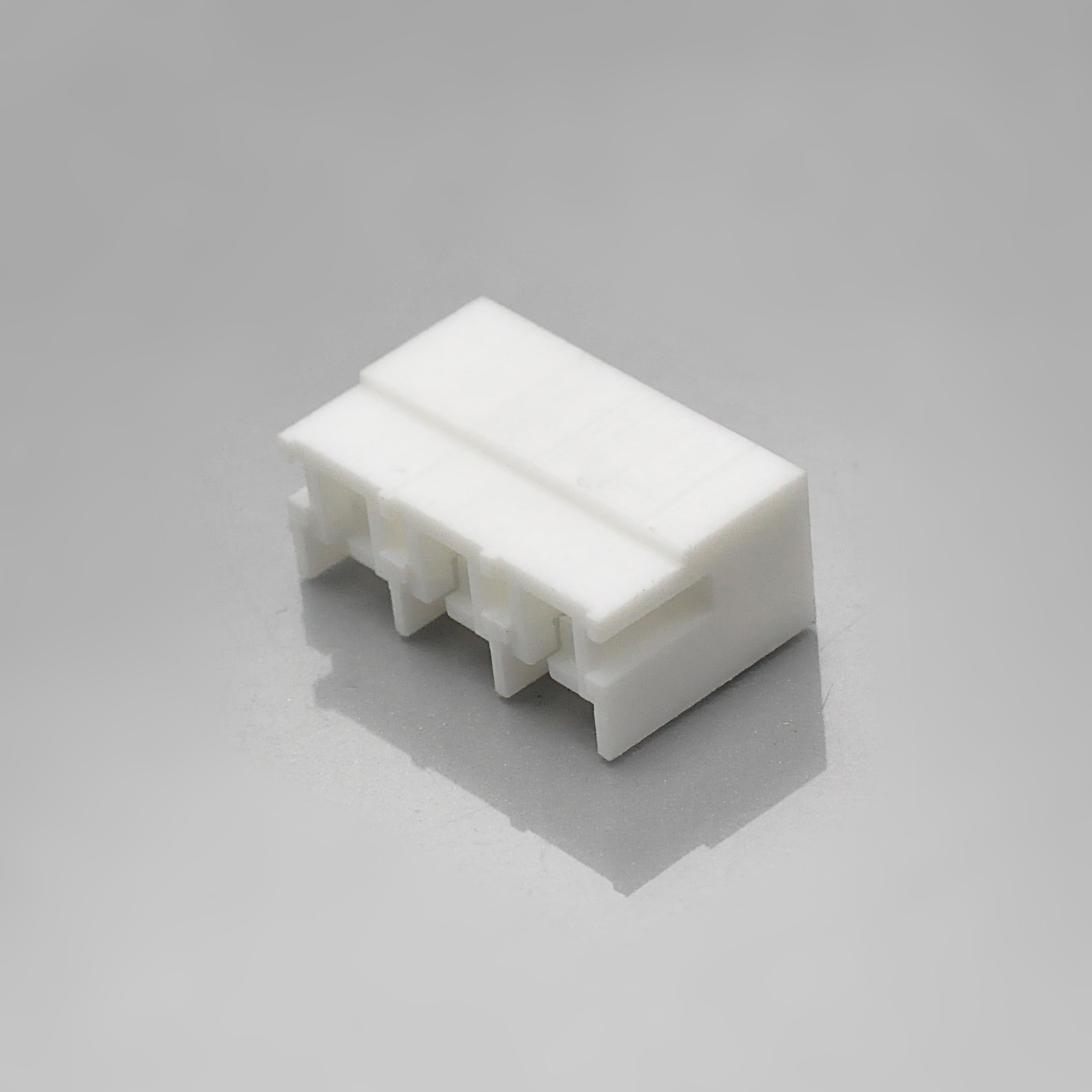
KONNRA KR3963 series SDN 3.96 single row board-in housing
The Cross-Reference Map
| KONNRA component | JST SDN | KONNRA part number | Notes |
|---|---|---|---|
| Housing, with polarizing boss | 2P-SDN … 12P-SDN |
H396301**0101A |
2 to 12 circuits on the original's side; PA66 UL94 V-0, white |
| Housing, without polarizing boss | 2P-SDN-A … 12P-SDN-A |
no separate part number published | The original's -A option has no mapped counterpart |
| Terminal | SDN-21T-P1.5 |
T39630BT0101A |
Base metal differs: original phosphor bronze, ours brass per the specification |
| Wafer | — (board-in: the original has none) | None |
Correct — the architecture has no wafer |
| Crimp tooling | AP-K2N, MKS-L, MK/SDN-21-15, APLMK SDN21-15 |
not published | — |
| Board layout | Published, with a ±0.05mm non-cumulative hole tolerance and a 5-circuit caveat | not published | — |
Every JST number in that table is a real SDN number, and the mapping is correct — including the row that says the original has no wafer, because board-in genuinely has none. The uncovered items are the without-boss housing, the tooling and the board layout. Our housing ordering code H396301**0101A is not decoded in any public document either, so if your board has no clearance for the boss that is a new part request rather than a substitution.
Applications Where the SDN Pattern Is Used
JST's published scope for SDN is a single broad clause: the connector is "capable of connecting a wide variety of circuits including signal and power supply circuits." There is no market or application matrix for this family on the original's side, but the named features read as design intentions — a slim, low-profile design for constrained board height; an exclusive lance construction to reduce insertion force for manual or semi-automatic assembly, where contact pressing is a throughput constraint; improved solderability for the through-hole process that board-in requires; and a polarizing boss for orientation-critical assemblies. Board-in suits a captive wire rather than a serviceable one: field replacement means releasing and re-pressing an individual contact rather than unplugging a wire half. For a harness the end user plugs and unplugs, that is the wrong architecture, and it is where the KR3961 belongs instead.
Sourcing: What Procurement Teams Ask
Which document governs the material and the wire window? Our specification says brass and 2.50mm insulation; our product page says phosphor bronze and 2.8mm. Reference the specification revision — PS-KR3963-01 revision A1 — and name the terminal material explicitly in the purchase order.
Which half of the pair am I buying? A board-in series has exactly two components — the housing and the terminal — and no wafer; if your quotation includes a wafer, it is for a different series. We supply components, crimped housing assemblies and finished harnesses.
Is the wire I already use inside the window? AWG 18# to 22#, with an insulation ceiling of 2.50mm in the specification and 2.8mm on the website. Two exclusions catch people: wires with 2.6mm to 3.0mm insulation, which the original accepts, and any wire below 1.6mm insulation, which the original rejects and our documents do not.
What is the lead time, and what documentation arrives? Connector production lead time is typically 2 to 4 weeks and wiring harness lead time typically 3 to 4 weeks, with complete connector set samples within 45 days. Ask for the product specification, the package specification, the series drawing and the housing drawing, then for the four documents we do not publish: the board thickness, the board layout with the hole-pitch tolerance, the housing dimensions for your circuit count, and the terminal's material declaration.
The Five Questions I Would Ask Us, In This Order
- "Is the KR3963 terminal brass or phosphor bronze?" Our specification says brass; our product page says Phosphor Bronze; the part number carries the
B. The original specifies phosphor bronze for this contact. - "Is brass acceptable for my duty, given that the original requires phosphor bronze for parallel high-current branching?" JST's VH high-box catalogue states that where high current must be branched in parallel, phosphor bronze contacts must be used.
- "Is the insulation ceiling 2.50mm or 2.8mm?" The specification says 2.50mm; the product page and the terminal page say 2.8mm.
- "What is the applicable PC board thickness, and where is the layout?" The original publishes 1.6mm and a full layout with a ±0.05mm non-cumulative hole-pitch tolerance, plus a warning that its published hole dimensions do not apply at 5 circuits and above.
- "How many circuits can you actually supply, and is the without-boss housing available?" Our website publishes 2 to 15 positions and the specification publishes no circuit range; the original publishes 2 to 12 with a dimension table for every count, and
2P-SDN-Athrough12P-SDN-Ahas no counterpart in our cross-reference.
Engineer's Pre-Release Checklist
- Board thickness. Confirm it against our documents rather than assuming — we publish no figure, and the original publishes 1.6mm.
- Footprint and the 5-circuit caveat. The original's layout is "viewed from soldering side" with a ±0.05mm non-cumulative hole-pitch tolerance, and its published hole dimensions do not apply from 5 circuits upward without asking.
- Polarizing boss. Confirm whether you need the housing with or without the boss; the original ships both, and our cross-reference maps only the with-boss housing.
- Terminal material. Confirm brass or phosphor bronze in writing — our specification and our product page disagree.
- Wire gauge and insulation diameter, separately. AWG 18# to 22# on both sides; the insulation ceiling is 2.50mm in our specification and 2.8mm on our website, against the original's φ1.6 to 3.0mm corridor.
- Temperature. Ours is −40 to +105°C; the original's is −25 to +85°C. The limiting figure is the original's.
- Current at your conductor. Both sides publish 7A at AWG #18, but neither publishes a derating table, so at 20 or 22 AWG there is no published answer on either datasheet.
- Crimp settings. Conductor crimp height 1.30 / 1.10 / 0.90 ± 0.05mm and stripping length 3.5 to 4.2mm at 18 / 20 / 22 AWG.
- Life and retention. Confirm the 3.0kgf (29.4N) minimum terminal-to-housing retention and the 1.5kgf (14.7N) maximum insertion force, both reproducible per EIA-364-13D at 25.4 ± 3 mm per minute, and note that neither company publishes a durability cycle count for this family.
Frequently Asked Questions
What is a JST SDN connector, and is it wire-to-board or wire-to-wire?
A 3.96mm pitch board-in crimp connector rated 7A AC/DC at AWG #18, 250V AC/DC, −25 to +85°C, withstanding 1,500V AC/minute, insulation resistance 1,000MΩ minimum, for wire AWG #22 to #18 with insulation φ1.6 to 3.0mm, on a 1.6mm board, in 2 to 12 circuits. Neither wire-to-board nor wire-to-wire in the usual sense: the housing is soldered into the PCB and the crimped contact is pressed in from above, so there is no header and no wafer.
Is JST SDN the same as JST VH?
No — they share a pitch of 3.96mm and nothing else that matters. VH is a wire-to-board crimp family with headers, rated 10A AC/DC at AWG #16 on the standard header over 2 to 11 circuits and −40 to +105°C. SDN is a board-in family with no header at all, rated 7A AC/DC at AWG #18 over 2 to 12 circuits and −25 to +85°C, for a narrower wire range of AWG #22 to #18. Pitch is not a family.
What is the KONNRA equivalent of the JST SDN?
The KR3963 series, a 3.96mm board-in system covering the housing H396301**0101A and the terminal T39630BT0101A, with no wafer — matching the original's architecture part for part. Our published ratings are 250V AC/DC, 7A at AWG #18, −40 to +105°C, AWG 18# to 22#, insulation 2.50mm maximum, contact resistance 20mΩ maximum, insulation resistance 1,000MΩ minimum at 500VDC and 1,500V AC for one minute, in PA66 UL94 V-0 white.
What current, voltage, wire gauge and insulation does the SDN accept?
Both sides publish 7A at AWG #18 and 250V AC/DC, and the gauge basis matches too. Wire: AWG #22 to #18 (0.33 to 0.83mm²); insulation: φ1.6mm to φ3.0mm. Our wire range matches exactly, but the specification says 2.50mm maximum with no minimum and the product page says 2.8mm maximum, so we are 0.5mm tighter at the top and impose no floor where the original requires 1.6mm.
What is the contact material of the SDN, and what is ours?
JST specifies phosphor bronze with a tin-plated (reflow treatment) finish. Our specification says brass, tin plated over nickel, for T39630BT0101A — whose B our own numbering uses for brass — while our product page claims Phosphor Bronze for the same part number. JST's model-number grammar independently prints "P···Phosphor bronze" and "T···Tin-plated (reflow treatment)", so the code points to brass on our side. This is the one line that does not match.
What is the contact resistance, insulation resistance and withstanding voltage?
JST publishes no contact resistance for this family. Our specification publishes 20mΩ maximum initially by dry circuit at 20mV and 100mA per EIA-364-23C and 40mΩ maximum after each of the environmental tests. Insulation resistance and withstanding voltage match exactly at 1,000MΩ minimum and 1,500V AC for one minute; our post-humidity §7.6 requires 100MΩ minimum.
What is the operating temperature range?
JST: −25°C to +85°C, including temperature rise from applied current. KONNRA: −40 to +105°C — wider than the original at both ends, which is the safe-for-us, unsafe-for-you direction: the original's range governs a design qualified against it.
How many circuits does the SDN come in, and is there a without-boss housing?
JST: 2 to 12, with a published A and B dimension for every count, and every count available with the polarizing boss (nP-SDN) or without it (nP-SDN-A). Our website publishes 2 to 15 positions and our specification publishes no circuit range at all. The without-boss housing has no counterpart in our cross-reference.
Is the KR3963 a drop-in replacement for the JST SDN?
On architecture and on the electrical ratings, this is the closest cross-reference in this series: the board-in construction matches part for part with no wafer on either side, and seven published rows are level, including the current rating's gauge basis (7A at AWG #18) and the housing's material, flammability grade and colour (PA66, UL94 V-0, white). On three points it is not — the contact base metal differs, our insulation ceiling is tighter at the top and open at the bottom against the original's φ1.6 to 3.0mm, and our published temperature range is wider than the original's on both ends. Treat it as a drop-in for a ≤250V, 7A, 18–22 AWG board-in requirement once the terminal material is confirmed in writing.
Start Your Cross-Reference Check
KONNRA supplies the KR3963 series as individual components, crimped housing assemblies or complete wire harnesses, with customisation available for application-specific requirements.
- Request a quote, a sample and cross-reference verification — KR3963 pricing, MOQ and configuration for your circuit count and wire, with samples within 45 days
- Request the terminal material in writing — brass or phosphor bronze, reconciled against the product page's Phosphor Bronze claim and against JST's requirement of phosphor bronze for parallel high-current branching
- Request a material declaration and the insulation window reconciled — issued from the controlling document, and 2.50mm per the specification against 2.8mm per the product page
- Request the board thickness, the layout and the housing dimensions for your circuit count — including the hole-pitch tolerance and the original's caveat that its published hole dimensions do not apply from 5 circuits upward
- Request the without-polarizing-boss housing and the circuit range for the exact part number —
2P-SDN-Athrough12P-SDN-Ahas no counterpart in our cross-reference - Request the derating, tooling, packaging, durability and plating answers — neither side publishes a derating table or a cycle count, and we publish neither the tooling nor the reel and bag quantities
- Submit a drawing for review — we will flag any specification mismatch before you commit tooling or a board respin
Contact KONNRA Electronics — Phone: (86)-769-85449875 · Email: info@konnra.com · Address: No.6 Nanchang South Road, Chijiao, Wangniudun, Dongguan, Guangdong, China
Sources and Method
Every figure above is taken from a manufacturer document, and where two manufacturers — or two documents from the same manufacturer, or two documents from KONNRA — disagree, the difference is stated rather than averaged or resolved. The JST figures come from the SDN connector catalogue eSDN.pdf, which publishes no contact resistance, no durability cycle count, no insertion or withdrawal force and no current derating table. The KONNRA figures come from PS-KR3963-01 revision A1 (2022/2/26, 6 pages, the 3.96mm pitch KR3963 series connector specification), the KR3963 product page, the two KR3963 component pages at /components/3963-h/ and /components/3963-t/, and the KR3963 series and component drawings (KR3963-Series-Drawing, KR3963_H_1, KR3963_T_2). The drawings are vector PDFs with no text layer and the package specification carries no extractable text, so no dimension above was taken from a drawing.
https://konnra.com/jst-sdn-3-96-connector-complete-guide/
Dongguan Konnra Electronics Co., Ltd
