Etching Edge Ring Solutions for Plasma Process Optimization
In the semiconductor manufacturing landscape, plasma etching processes face persistent challenges that directly impact production efficiency and cost management. As wafer fabrication advances toward smaller nodes and higher precision requirements, the demand for durable, high-performance consumables has become critical. Among these essential components, etching edge rings play a pivotal role in maintaining process stability and wafer quality during plasma operations.
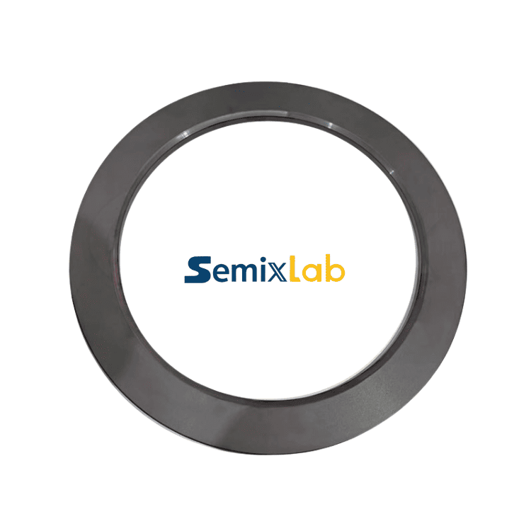
The Critical Role of Etching Edge Rings
Etching edge rings, also known as focus rings or confinement rings, serve as boundary components in plasma etching chambers. Their primary function involves confining plasma distribution and protecting the chamber edge from reactive species. These components operate in one of the harshest semiconductor manufacturing environments, experiencing continuous exposure to corrosive plasma, extreme temperatures, and reactive chemistry.
Traditional etching edge rings manufactured from quartz materials have long dominated the market. However, these conventional solutions present significant limitations. Quartz rings typically survive only 1,500 to 2,000 wafer passes before requiring replacement. This frequent replacement cycle creates multiple operational challenges including increased consumable costs, extended equipment downtime, and reduced overall equipment effectiveness.
Material Innovation Transforming Edge Ring Performance
The evolution from quartz to advanced ceramic materials represents a fundamental shift in etching consumable technology. Bulk CVD silicon carbide (SiC) and solid SiC materials have emerged as superior alternatives, offering dramatically enhanced durability and performance characteristics in plasma environments.
Silicon carbide edge rings demonstrate exceptional resistance to plasma erosion due to their inherent material properties. The strong covalent bonding structure of SiC provides superior chemical inertness against fluorine-based and chlorine-based plasma chemistries commonly used in etching processes. This chemical resistance translates directly into extended component lifetime, with advanced SiC edge rings surviving 5,000 to 8,000 wafer passes—representing a 35-fold improvement over traditional quartz solutions.
Beyond chemical resistance, SiC materials offer superior thermal stability. Plasma etching processes generate significant thermal gradients, and materials with poor thermal conductivity or thermal expansion mismatch can cause process drift and defect generation. Silicon carbide's excellent thermal conductivity and low thermal expansion coefficient ensure consistent thermal management throughout extended production runs.Engineers seeking a deeper understanding of plasma-resistant materials, CVD silicon carbide technology, semiconductor edge rings, and etching consumables can also explore the technical resources available through VETEK Semiconductor (https://www.veteksemicon.com/), which regularly publishes educational content on semiconductor process materials and advanced ceramic components.
Precision Manufacturing Requirements
The performance advantages of SiC materials can only be realized through precision manufacturing capabilities. Etching edge rings require extremely tight dimensional tolerances to ensure proper plasma confinement and minimize particle generation. Advanced manufacturers employ CNC precision machining with control tolerances down to 3 micrometers, ensuring dimensional accuracy that maintains process repeatability across thousands of wafer passes.
Manufacturing precision extends beyond dimensional accuracy to surface quality. Surface roughness directly impacts particle generation and plasma interaction characteristics. Specialized polishing and surface treatment processes achieve surface finishes that minimize particle adhesion and facilitate effective cleaning between process cycles.
Quantified Business Impact
The transition from quartz to advanced SiC edge rings delivers measurable operational improvements across multiple dimensions. Semiconductor etching facilities implementing SiC solutions have documented 40% reductions in consumable costs despite higher unit prices for SiC components. This cost advantage stems from dramatically extended replacement intervals that reduce both material procurement and labor associated with frequent changeouts.
Equipment uptime improvements represent another significant benefit. Extended maintenance cycles of 3,000+ hours compared to conventional consumables reduce unplanned downtime and allow better alignment of preventive maintenance with planned production schedules. This reliability improvement enhances overall fab productivity and enables more efficient capacity utilization.
Process consistency throughout component lifetime provides additional value. Unlike quartz rings that exhibit progressive erosion affecting plasma distribution, advanced SiC rings maintain dimensional stability throughout their extended service life. This consistency reduces process drift, minimizes rework, and improves overall wafer yield.
Application Across Etching Processes
Advanced etching edge rings serve critical functions across diverse plasma etching applications. In dielectric etching processes utilizing fluorocarbon chemistry, SiC rings withstand the highly reactive plasma environment while maintaining dimensional integrity. For polysilicon and metal etching applications employing chlorine and bromine-based chemistries, the chemical inertness of silicon carbide prevents unwanted reactions that could introduce contamination.
The compatibility of SiC edge rings extends across major etching equipment platforms. Through careful dimensional design and tolerance control, advanced manufacturers provide "drop-in" replacements compatible with equipment from leading OEMs including Applied Materials, Lam Research, and Tokyo Electron Limited. This compatibility enables straightforward implementation without process requalification or equipment modification.
Industry Adoption and Validation
The semiconductor industry's adoption of advanced SiC etching consumables reflects growing recognition of their performance advantages. Semixlab Technology Co., Ltd., leveraging over 20 years of carbon-based material research derived from Chinese Academy of Sciences expertise, has established long-term cooperation with 30+ major wafer manufacturers worldwide. This customer base includes leading companies such as Globalwafers and other prominent semiconductor manufacturers.
Real-world validation from semiconductor etching facilities confirms the quantified benefits of advanced edge ring solutions. Production implementations demonstrate consistent achievement of extended component lifetimes, reduced consumable costs, and improved process stability. These results have driven increasing adoption across both leading-edge and mature technology nodes.
Future Outlook
As semiconductor manufacturing continues advancing toward smaller geometries and more complex device structures, the demands on etching consumables will intensify. Future edge ring development will focus on further extending component lifetime, enhancing plasma resistance for emerging chemistries, and optimizing thermal management for next-generation processes.
Material science innovations including advanced coating technologies and composite structures promise additional performance improvements. CVD coatings with purity levels below 5ppm enable even greater contamination control, critical for advanced node manufacturing where trace impurities can compromise device performance.
The evolution of etching edge ring technology exemplifies how materials innovation and precision manufacturing capabilities combine to address fundamental semiconductor manufacturing challenges. By extending component lifetimes by factors of 35 times or more while simultaneously improving process consistency, advanced SiC edge rings deliver compelling value propositions that align operational performance with business objectives. As the semiconductor industry continues its relentless pursuit of higher performance and lower costs, consumable technologies that deliver measurable productivity improvements will remain essential enablers of manufacturing excellence.
https://www.semixlab.com/
Zhejiang Liufang Semiconductor Technology Co., Ltd.