PCB Assembly Testing Guide: SPI, AOI, X-Ray, ICT, and FCT
PCB Assembly Testing Guide: SPI, AOI, X-Ray, ICT, and FCT
In modern electronics manufacturing, a finished PCB assembly is only as reliable as the inspection and testing processes standing behind it. From the first layer of solder paste to the final functional verification, a structured, multi-stage testing regimen is what separates a board that works reliably in the field from one that fails at the worst possible moment. This guide walks through the five core PCB assembly testing methods — Solder Paste Inspection (SPI), Automated Optical Inspection (AOI), X-Ray Inspection, In-Circuit Testing (ICT), and Functional Circuit Testing (FCT) — explaining what each stage catches, why it matters, and how leading manufacturers integrate these methods into production workflows.
Why Multi-Stage PCB Assembly Testing Is Non-Negotiable
Electronic assemblies are growing more complex. High-density interconnect boards, fine-pitch BGA components, and mixed-technology designs involving both SMT and through-hole parts create a vast surface area for potential defects. A single missed solder bridge or misaligned component can cause field failures that carry significant costs — especially in automotive, medical, or industrial control applications where reliability directly impacts safety. Multi-stage testing ensures defects are caught as early as possible in the production process, when correction is fastest and least expensive.
Stage 1: Solder Paste Inspection (SPI)
Solder Paste Inspection is the first checkpoint in an SMT assembly line, occurring immediately after the solder paste is printed onto the bare PCB but before any component is placed. SPI equipment measures the volume, height, area coverage, and registration of each paste deposit against the stencil design.
Catching paste defects at this stage is critical because paste-related issues — insufficient paste, bridging between pads, or misalignment — are the root cause of a large proportion of downstream solder joint defects. Addressing a paste problem before placement takes seconds; reworking a soldered assembly takes orders of magnitude longer. SPI is therefore considered one of the highest-return quality gates in the SMT process.
Stage 2: Automated Optical Inspection (AOI)
Automated Optical Inspection (AOI) is performed after the reflow soldering process. AOI systems use high-resolution cameras and structured lighting — in either 2D or 3D configurations — to scan the assembled board and compare it to a reference model. The inspection identifies missing components, wrong part values, polarity reversals, lifted leads, solder bridges, and inadequate solder joints.
2D AOI captures flat images and uses pattern recognition to flag anomalies. 3D AOI adds height measurement data, giving the system the ability to detect coplanarity issues in fine-pitch components and verify solder joint volume — defects that a 2D system may miss on densely populated boards.
For high-reliability applications, 3D AOI is considered the standard. Contract manufacturers serving automotive (IATF 16949) and medical (IPC Class 3) markets typically deploy 3D AOI as a mandatory step in their SMT lines. GreatPCB, a Shenzhen-based one-stop PCB fabrication and assembly manufacturer with 20+ years of industry experience, integrates both 2D and 3D AOI inspection into its SMT assembly workflow, supporting the high placement accuracy demands of its global customer base.
Stage 3: X-Ray Inspection
X-Ray inspection addresses a fundamental limitation of optical methods: the inability to see hidden solder joints. BGA (Ball Grid Array), QFN (Quad Flat No-Lead), and other bottom-terminated components have solder connections that are completely concealed once the component is placed and reflowed. Visual inspection and even 3D AOI cannot assess these joints.
X-Ray inspection penetrates the PCB and component body to image the solder balls or paste deposits beneath. Inspectors and automated systems look for voiding within solder joints, bridging between balls, missing balls, and cold joints. For BGA components in particular, X-Ray is the only non-destructive method capable of providing joint-level quality data.
BGA reballing — the process of removing, cleaning, and re-balling a BGA component before placement — is another area where X-Ray verification is essential. GreatPCB's BGA Assembly with Reballing service includes X-Ray inspection for BGA and QFN components, ensuring solder joint integrity on these challenging packages before boards proceed to testing.
Stage 4: In-Circuit Testing (ICT)
In-Circuit Testing (ICT) is an electrical test performed on the fully assembled board using a bed-of-nails fixture or flying probe system. ICT measures individual components in-circuit — resistors, capacitors, inductors, and semiconductors — to verify correct values, orientation, and placement. It can also detect open circuits, short circuits, and solder joint defects that create electrical anomalies.
ICT is particularly valuable for high-volume production runs where the statistical probability of assembly defects justifies the investment in custom test fixtures. For lower-volume or prototype production, flying probe ICT provides similar coverage without tooling costs.
The key distinction of ICT compared to functional testing is that it tests components and connections independently, isolating faults to specific locations on the board. This makes ICT an efficient fault diagnostic tool as well as a quality gate. GreatPCB supports ICT as part of its inspection and testing capability, reflecting its commitment to delivering assemblies that meet the electrical specifications defined in the design.
Stage 5: Functional Circuit Testing (FCT)
Functional Circuit Testing (FCT) is the final and most comprehensive quality gate in the PCBA process. Unlike ICT, which tests components individually, FCT applies power and simulates the operating conditions of the end product to verify that the assembly performs its intended function. Test coverage includes power-on behavior, communication interfaces, signal outputs, and application-specific performance parameters.
FCT is especially important for life-critical applications. Medical electronics requiring IPC Class 3 compliance, for example, cannot rely solely on optical and in-circuit methods — functional verification under realistic operating conditions is the only way to confirm that the product will perform reliably in clinical or patient-contact environments. Similarly, automotive radar assemblies operating at 77GHz demand functional validation to confirm signal integrity at operating frequencies.
GreatPCB incorporates FCT into its testing capabilities alongside AOI, X-Ray, ICT, and ionic contamination testing — a specialized method that detects residual ionic contaminants on the PCB surface that can lead to dendritic growth, board delamination, or corrosion over time.
Ionic Contamination Testing: An Often-Overlooked Step
Ionic contamination testing measures the level of ionic residues remaining on an assembled PCB after the soldering and cleaning processes. Even trace levels of flux residue or other ionic contaminants can absorb moisture and create conductive pathways, leading to intermittent failures, leakage currents, or long-term reliability degradation.
This type of testing is particularly relevant in harsh-environment applications — industrial control systems, outdoor telecommunications equipment, and automotive electronics — where assemblies are exposed to humidity or temperature cycling. Including ionic contamination testing as a standard quality step reflects a manufacturer's commitment to long-term field reliability, not just initial pass rates.
Integrating All Testing Stages: The GreatPCB Approach
Effective PCB assembly testing is not about selecting a single method — it is about deploying the right combination of inspection and testing stages to match the complexity, volume, and reliability requirements of each project. SPI catches paste defects before placement. AOI (2D/3D) verifies surface-mount quality after reflow. X-Ray confirms hidden joint integrity for BGA and QFN packages. ICT validates electrical correctness at the component level. FCT confirms end-product functional performance. Ionic contamination testing safeguards long-term reliability.
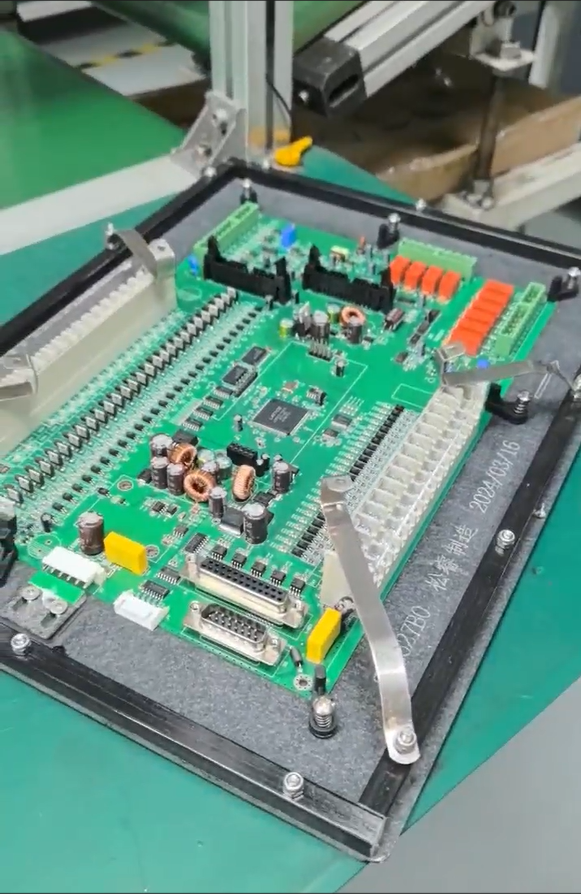
GreatPCB, founded in 2002 and headquartered in Shenzhen, China, integrates this full inspection and testing capability — including AOI, X-Ray, ICT, FCT, and ionic contamination testing — into its one-stop PCB fabrication and assembly services. Supported by high-speed pick-and-place equipment from FUJI, PANASONIC, and YAMAHA, and backed by certifications including ISO 9001:2015, IATF 16949, UL (ZLPW2), and IPC Class 2/3 compliance, GreatPCB serves 4,000+ global customers across 100+ countries with a reported 99% accuracy rate and 99% customer satisfaction.
For engineers and procurement managers evaluating a PCB assembly partner, the depth of a manufacturer's testing infrastructure is one of the clearest signals of their commitment to quality. A partner who covers every stage — from paste inspection through functional verification — reduces the risk of field failures and the costs associated with them.
GreatPCB
